ZEISS SEMs for Industry: Scanning electron microscopy portfolio
With its scanning electron microscopes, ZEISS offers a broad portfolio of systems for a variety of applications in the field of industrial quality assurance and failure analysis.
More information, more possibilities. SEM-Analyses for Industry.
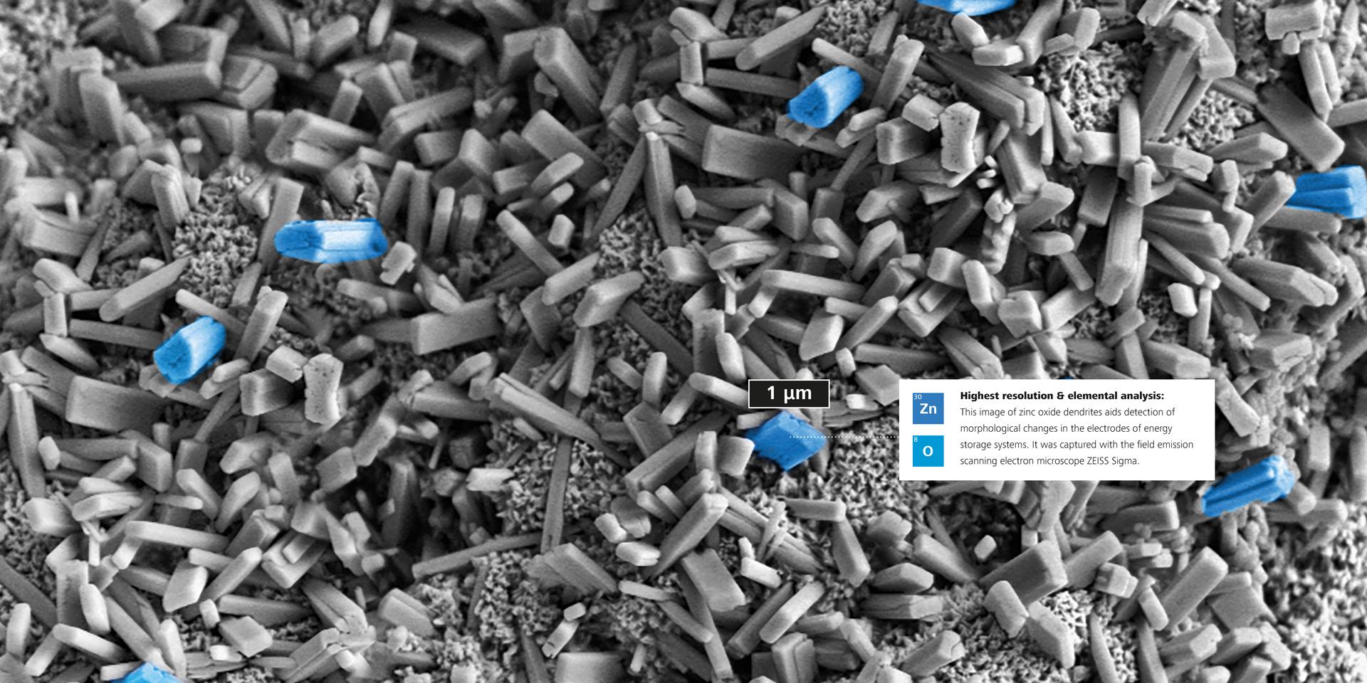
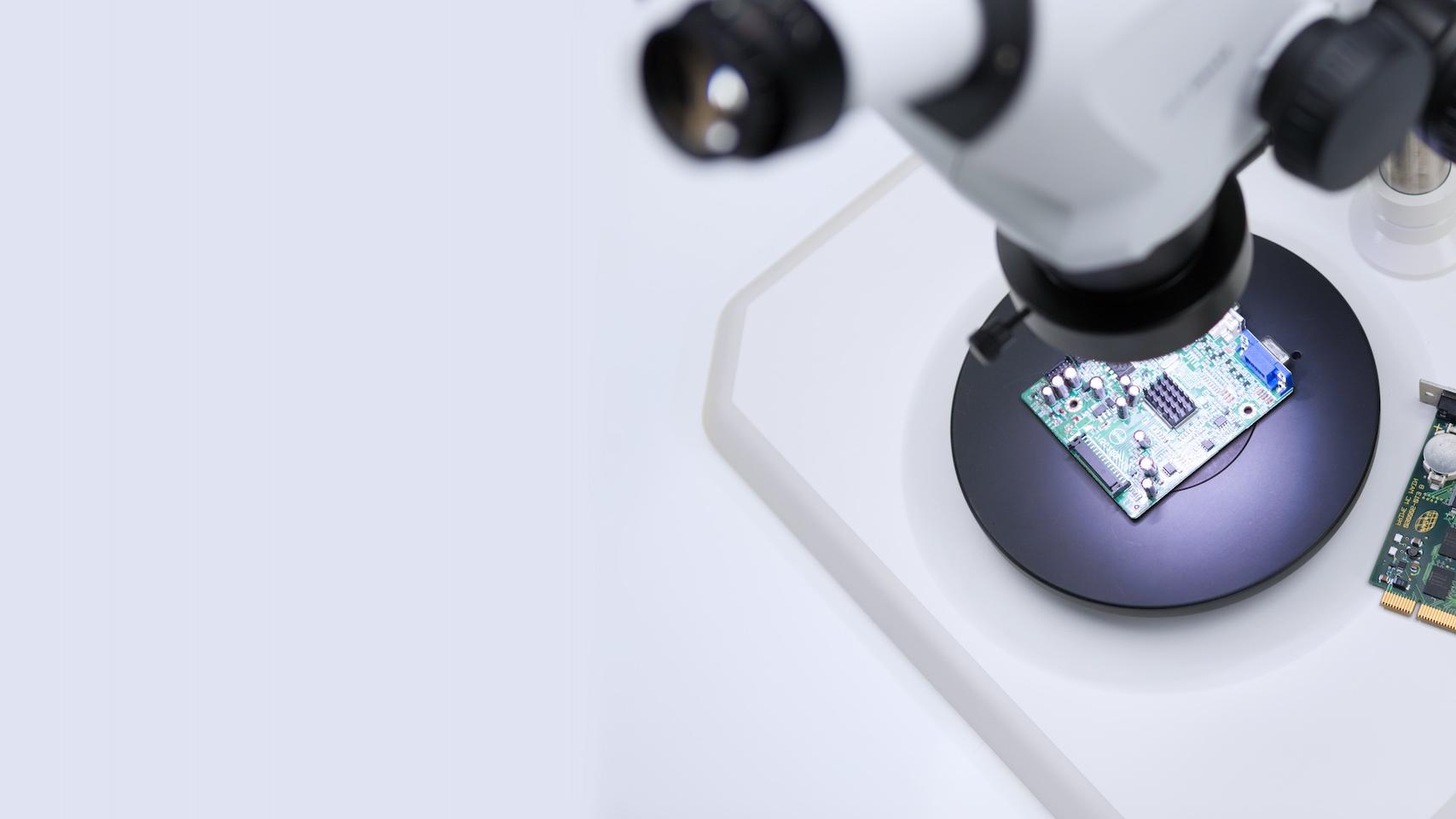
Scanning electron microscopy (SEM) is used for extremely precise component microstructure analysis featuring excellent depth of field and higher resolution. This method generates image captures of the sample surface with very high magnification. Energy-dispersive X-ray spectroscopy (EDS) can additionally be performed on the SEM, which enables the chemical element composition of materials to be determined.
The solutions to meet your needs
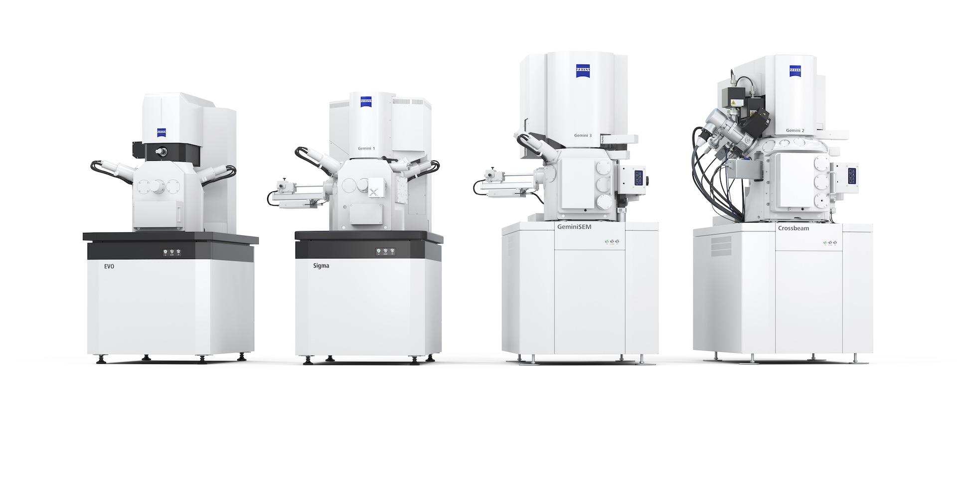
ZEISS scanning electron microscope (SEM) series
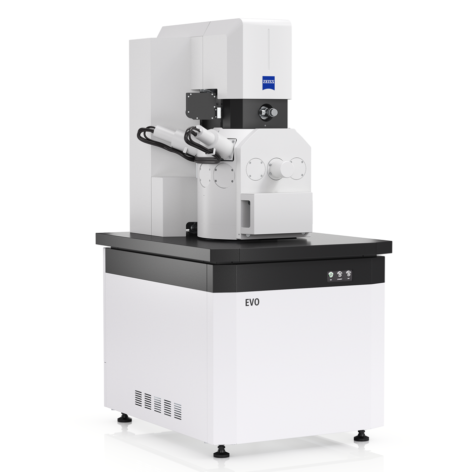
ZEISS EVO Family
Standard entry-level system
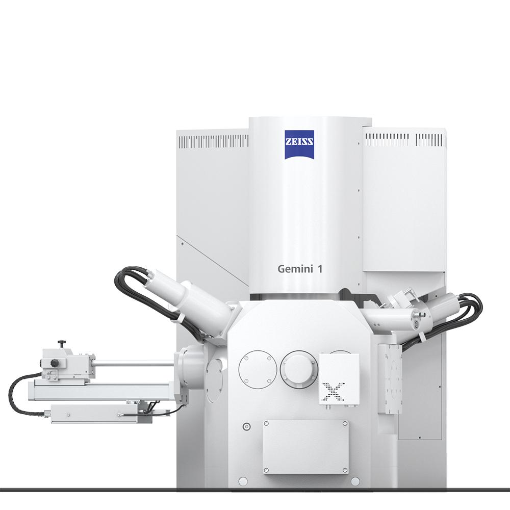
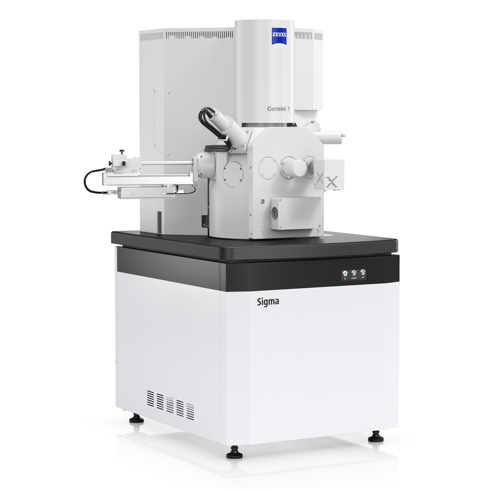
ZEISS Sigma Family
Advanced system
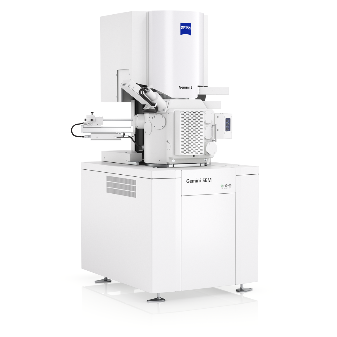
ZEISS GeminiSEM Family
High-End-System
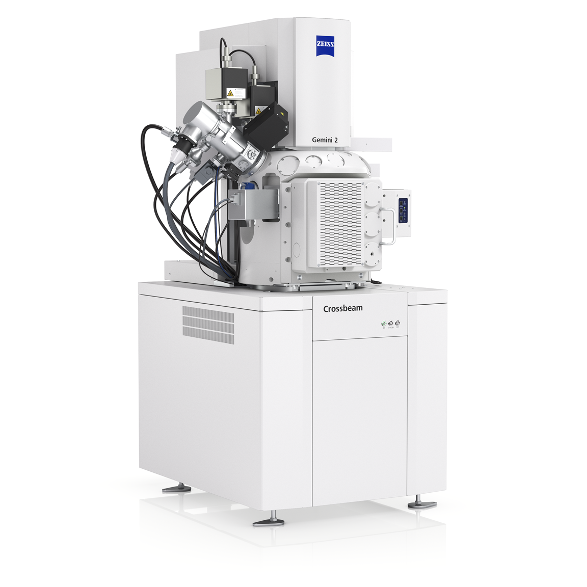
ZEISS Crossbeam Family
High-End-System with 3D Capability
Resolution
at 1 kV: 9 nm
at 1 kV: 1.3 nm
at 1 kV: 0,8 nm
at 1 kV: 1,4 nm
System
Conventional scanning electron microscope dedicated to challenging analytical EDS workflows with easy-to-use software options
Field emission scanning electron microscope for high-quality imaging and advanced analytical microscopy
Field emission scanning electron microscope for the highest demands in sub-nanometer imaging, analytics, and sample flexibility
Field emission scanning electron microscope for high-throughput 3D analysis and sample preparation and the use of a femtosecond laser
Benefits
Handles routine applications
Double condenser for best material feedback in your EDS routine
Flexible, powerful, and affordable
The smart alternative to tabletop SEMs for material analysis
Short time to result and high throughput
Accurate reproducible results from any sample
Quick and easy experiment setup
ZEISS Gemini technology
Flexible detection for clear images
Sigma 560 features best-in-class EDS geometry
Highest image quality and versatility
Advanced imaging modes
High-efficiency detection, outstanding analytics
ZEISS Gemini technology
Large variety of detectors for best coverage
Best 3D resolution in FIB-SEM analysis
Two beams, ions, and electrons
Sample preparation tool
Benefit from the additional femtosecond laser
EDS, EBSD, WDS, SIMS, plus more on request
Maximize sample insights through targeted analysis in the third dimension
Fast 3D failure analysis.correlative workflow solution from ZEISS.
Cross-scale material analysisin just four steps.
Localization and navigation on the SEM made easy: ZEISS ZEN Connect
Preparation and analysis of solid-state batteries with ZEISS Xradia, ZEISS Crossbeam, ZEISS Orion
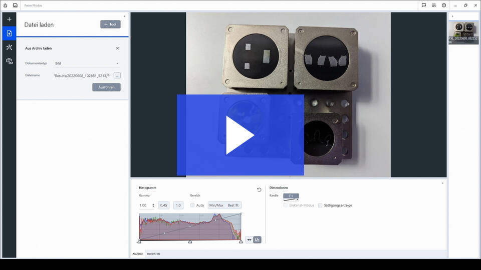
Third-party Content Blocked
The video player is blocked due to your cookie preferences. To change the settings and play the video, please click the button below and consent to use of "Functional" tracking technologies.
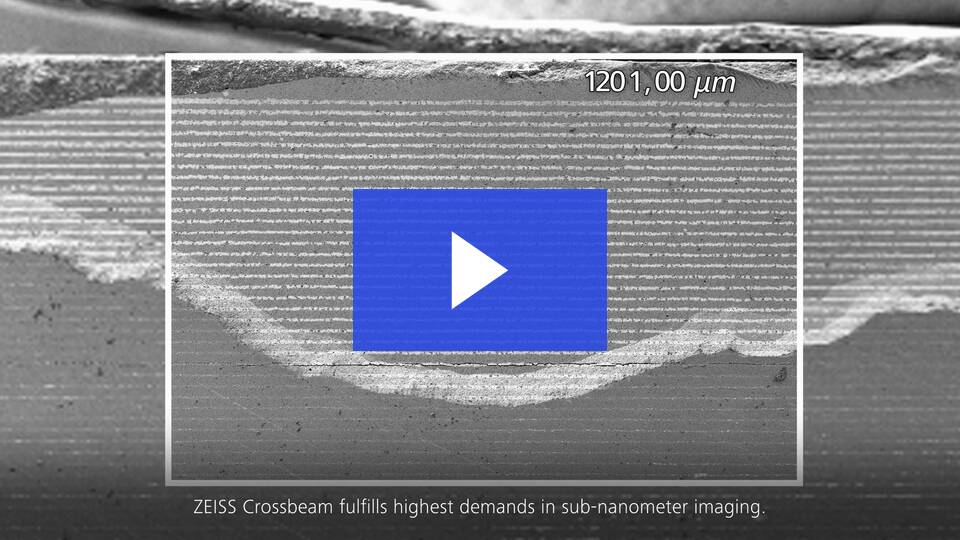
ZEISS Gemini technology for industry. ZEISS offers the right solution for every application. Watch the video to discover the development and benefits of Gemini technology.
The evolution of ZEISS Gemini optics
Third-party Content Blocked
The video player is blocked due to your cookie preferences. To change the settings and play the video, please click the button below and consent to use of "Functional" tracking technologies.
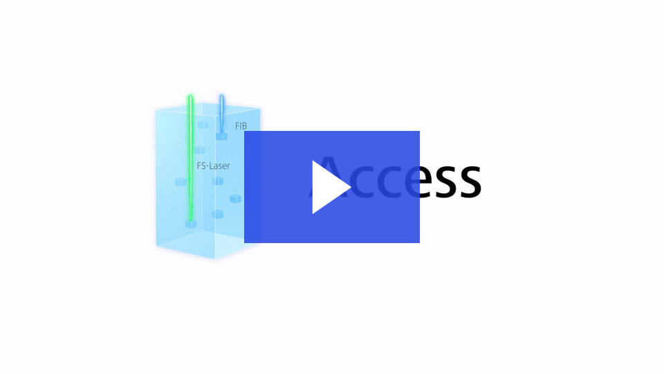
Watch the video about our correlative workflow solution! Learn how easy it is to use your data across technologies with ZEISS Solutions and how to achieve reliable and efficient results.
Fast 3D failure analysis.correlative workflow solution from ZEISS.
Third-party Content Blocked
The video player is blocked due to your cookie preferences. To change the settings and play the video, please click the button below and consent to use of "Functional" tracking technologies.
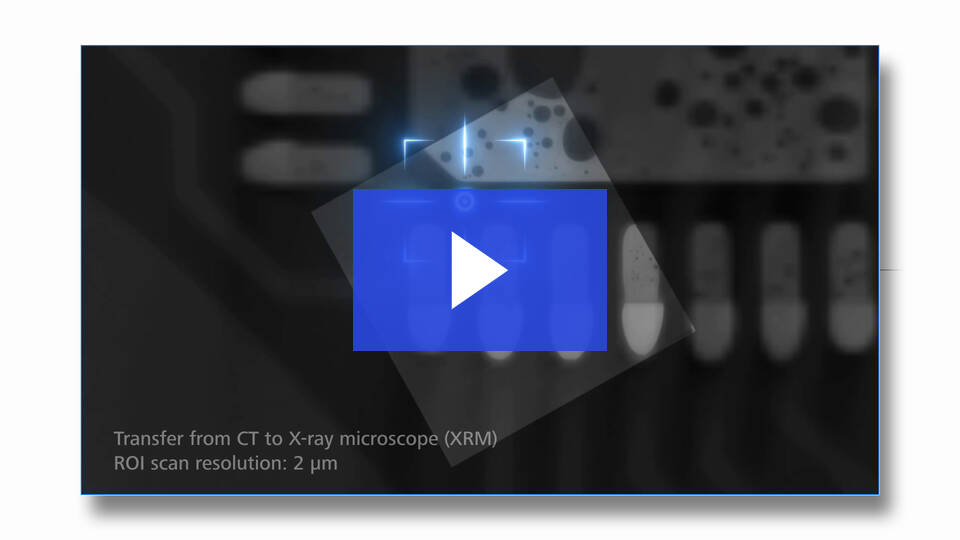
What do your macroscopic structures look like? How do you find the regions of interest in a large sample? How do you access these regions of interest (ROI)? And how do you analyze them further?
Cross-scale material analysisin just four steps.
Third-party Content Blocked
The video player is blocked due to your cookie preferences. To change the settings and play the video, please click the button below and consent to use of "Functional" tracking technologies.
Organize, visualize and contextualize different microscopy images and data of the same sample, all in one place. The correlation between images at different scales can be overlaid in the workspace and used for easy navigation.
Localization and navigation on the SEM made easy: ZEISS ZEN Connect
Third-party Content Blocked
The video player is blocked due to your cookie preferences. To change the settings and play the video, please click the button below and consent to use of "Functional" tracking technologies.
By inspecting intact samples, it is possible to determine changes in the composition that influence the quality and service life of batteries. ZEISS microscopy solutions for industry offer non-destructive and high-resolution 3D analyses as well as correlative analyses that are important for quality inspection.
Preparation and analysis of solid-state batteries with ZEISS Xradia, ZEISS Crossbeam, ZEISS Orion
ZEISS Efficient Navigation
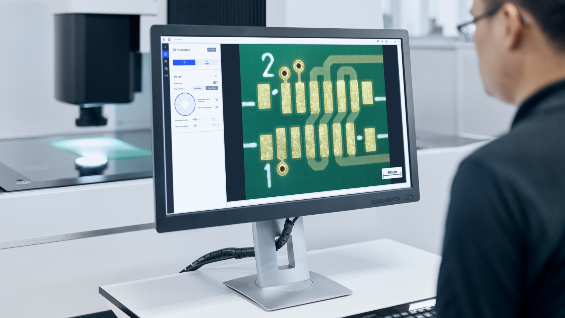
ZEISS ZEN core is your software suite for connected microscopy and image analysis. The software gives you a complete overview at a glance: It provides one user interface for all microscopy results.. Automated workflows at the push of a button ensure fast and reliable results.
A spotlight on correlative microscopy.
ZEISS ZEN Connect.
Organize and visualize different microscopy images to connect multimodal data - all in one place. This open platform enables you to quickly move from general overviews to advanced imaging, even when using third-party technology. With ZEN Connect, you can not only align, overlay and contextualize all image data. This allows you to easily transfer samples and image data between different light and electron microscopes.
ZEISS ZEN Connect enables
correlative image presentation from different microscope types (e.g. light and electron microscopes) in a connected map. This is highly beneficial for detailed investigation of large overview images, such as with battery cells. The module enables the import and correlation of non-image data such as EDS results. Compatible with the leading EDS system manufacturers.
A spotlight on correlative microscopy.
ZEISS ZEN Connect.
ZEN Connect provides you with a maximum of relevant data with a minimum of effort: All areas of interest are automatically retrieved after a one-time alignment and displayed in context. You can also organize data from multiple modalities. All images acquired with ZEN Connect can be saved in a well-structured database. Each image file is automatically given an individually predefined name. Each overlay image and its connected dataset is easy to find, and users can additonally search for microscope type via the new filter function.
Visualized data collection:
supports import and attachment of non-image data such as reports and descriptions (pdf, pptx, xlsx, docx, etc.).
Easy navigation:
click overview image to examine or re-evaluate any ROIs in full image overlay.
More intelligent. More time-saving.
ZEISS ZEN Intellesis.
Using established machine learning techniques such as pixel classification or deep learning, even non-expert users can achieve reliable, reproducible segmentation results with ZEISS ZEN Intellesis. Simply load your image, define your classes, label pixels, train your model and perform segmentation.
The software only needs to be trained once on a few images to be able to automatically segment batches of hundreds of images. This not only saves time, but also reduces the scope for user-related deviations. All time-consuming segmentation steps on the many similar images are handled by powerful machine learning algorithms.
ZEISS ZEN Intellesis
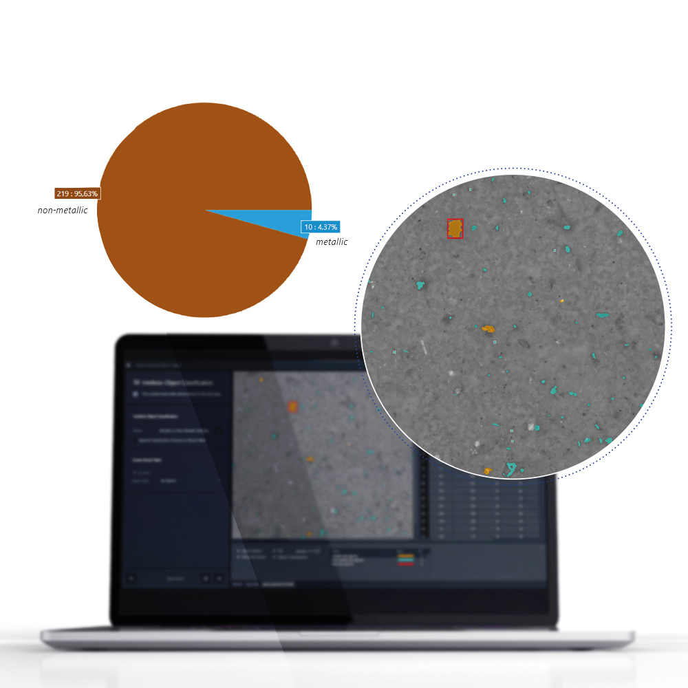
enables particle identification by machine learning and provides higher accuracy for particle identification, learning image segmentation, and object classification.
Intellesis Object Classification
is used to further classify segmented particles and sort these into their sub-types. This information can then be used to count particles per type.
More intelligent. More time-saving.
ZEISS ZEN Intellesis.
ZEN Intellesis supports easy segmentation of multidimensional images from numerous different imaging sources including widefield, super-resolution, fluorescence, label-free, confocal, light sheet, electron, and X-ray microscopy. ZEN’s evaluation modules then enable automatic report creation and measurement according to industrial standards.
When it comes to post-segmentation classification by type, ZEN Intellesis takes an innovative approach. Instead of looking at individual pixels as a typical machine learning solution would, its object classification model uses more than 50 measured properties per object to distinguish and classify them automatically. Based on tabulated data, this classification process is much faster than segmentation performed by specifically trained deep neural networks.
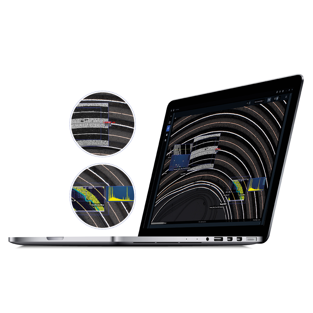
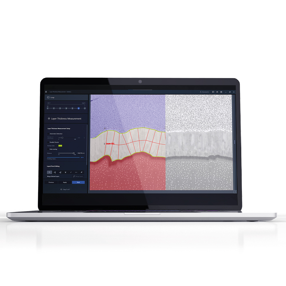
Example for layer thickness:
FIB cross section overlay of CIGS solar cell layers: result from Crossbeam 550 InLens detector (right) and after ZEN Intellesis machine learning segmentation (left).
We use ZEISS ZEN Intellesis for automatic segmentation and to better analyse the components of the second phase in dual-phase steel. The software changes the way we characterise materials and leads to faster and more reliable results.