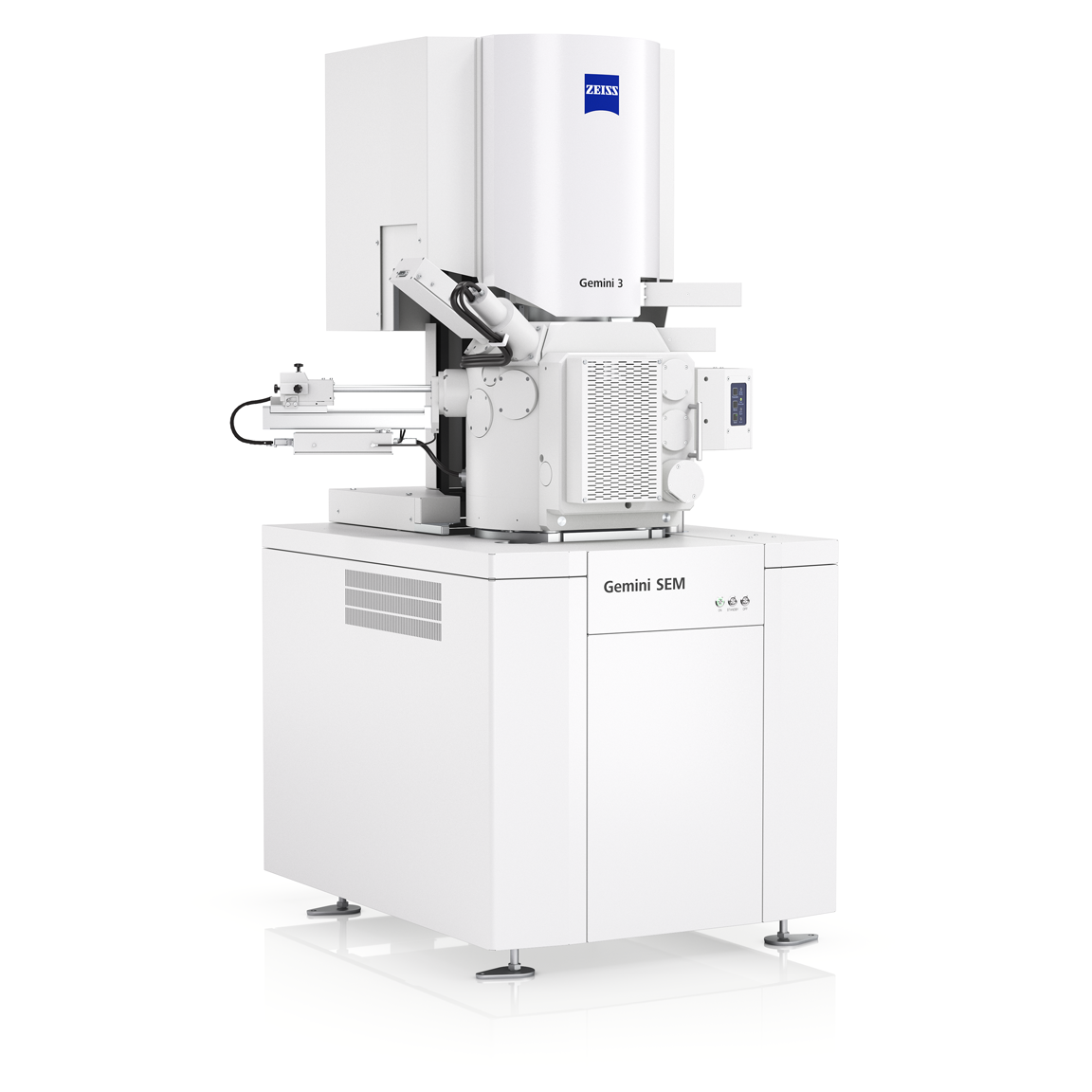
High-end field emission SEM ​

ZEISS GeminiSEM​

The class leader in sample flexibility​

Discover the unknown and meet the highest demands in sub-nanometer imaging, analytics, and sample flexibility with a field emission SEM.​ The system enables high throughput analysis while providing excellent resolution at low voltage, high speed, and high probe current.​

  • Highest image quality and versatility
  • Advanced imaging modes
  • High-efficiency detection, outstanding analytics 
  • ZEISS Gemini technology perfected over 25+ years
  • Large variety of detectors for best coverage

ZEISS GeminiSEM for industry​

Experience a new quality in the inspection of your samples.​

The system enables high throughput analysis while providing excellent resolution at low voltage, high speed, and high probe current. With its generous field of view and extremely spacious chamber, it is easy to examine even very large samples. ​

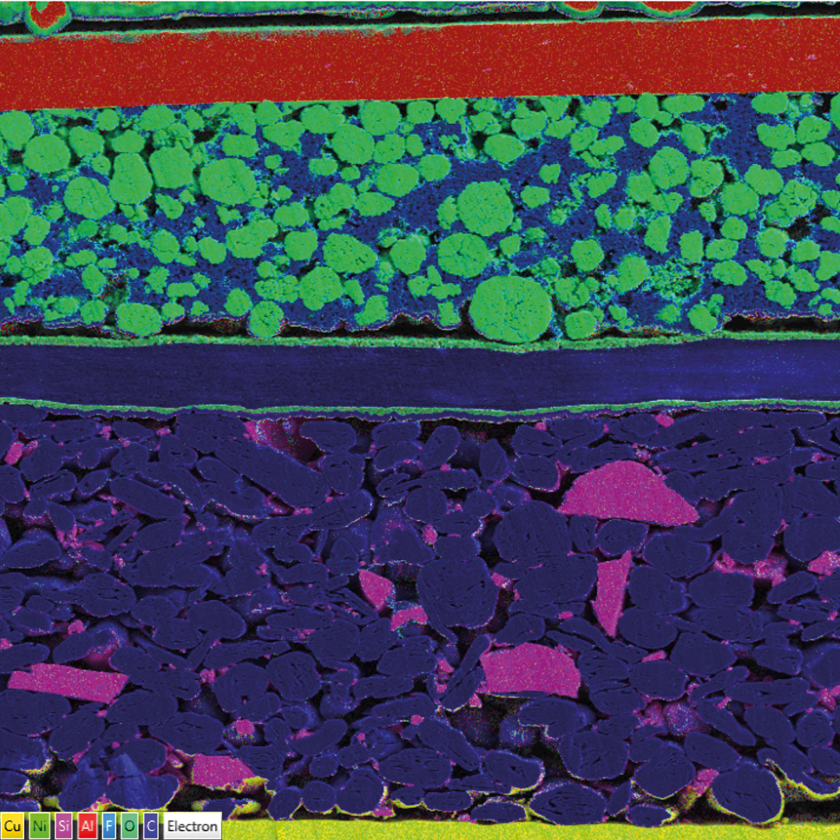
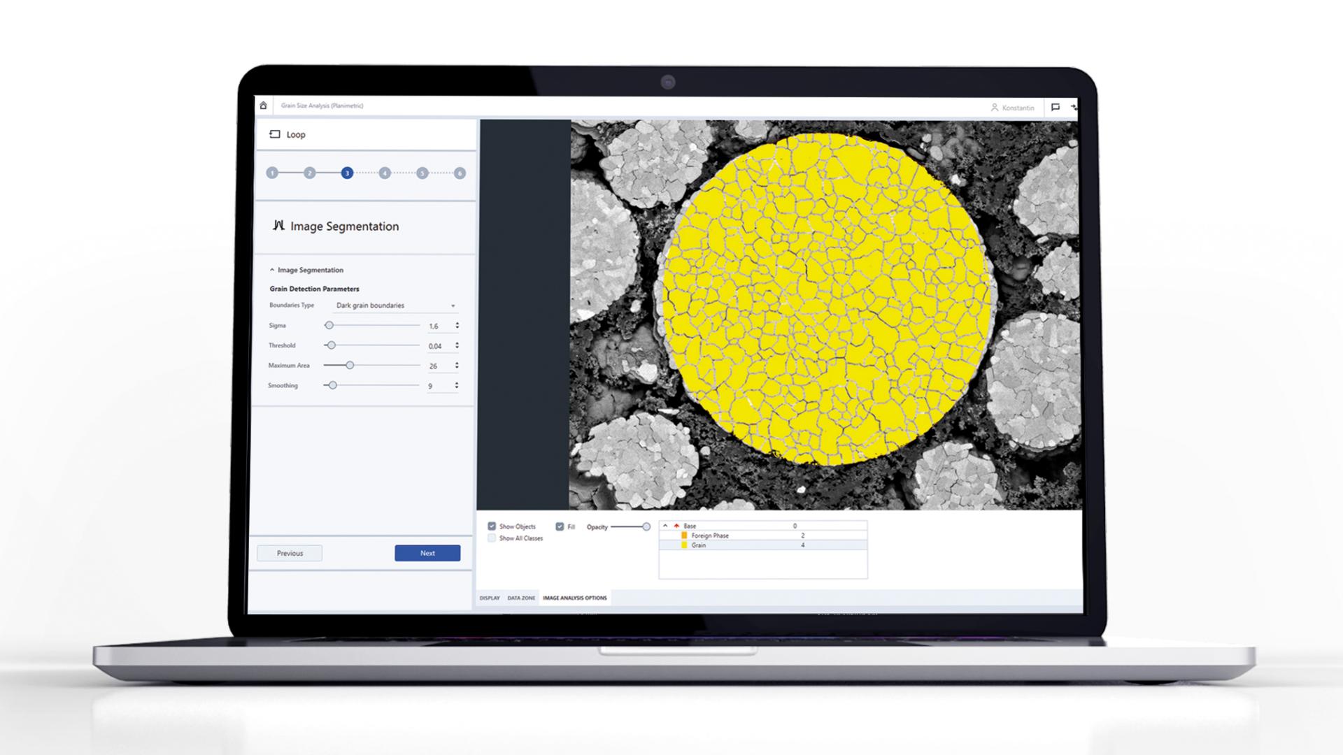
ZEISS GeminiSEM delivers efficient chemical composition and crystal orientation characterization with two diametrically opposed EDS ports and a coplanar EDS/EBSD configuration. Rely on shadow-free mapping at high speed. ​

Customize and automate your workflows: If you need to test materials to their technical limits, ZEISS puts an automated in-situ heating and mechanical stress lab at your disposal. ​

Fields of application at a glance

  • Failure analysis on mechanical, optical, and electronic components​
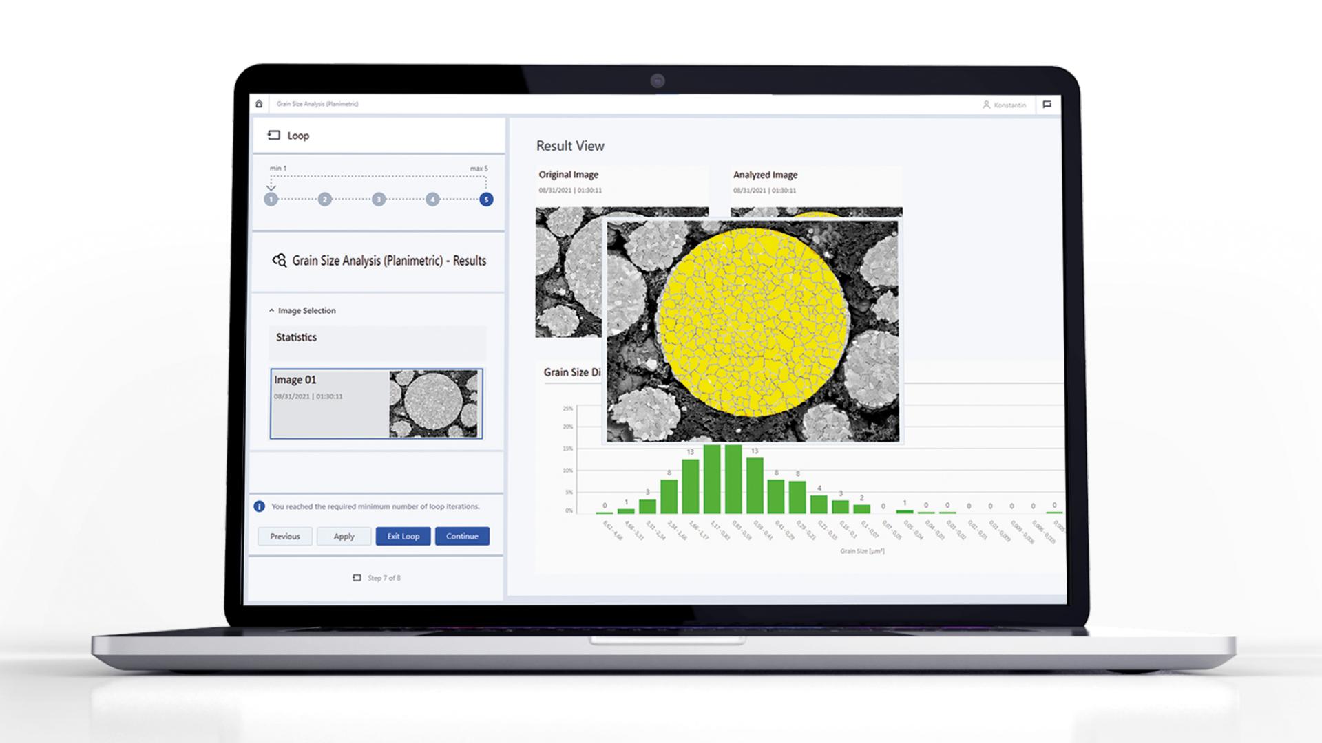
  • Fracture analysis and metallography​
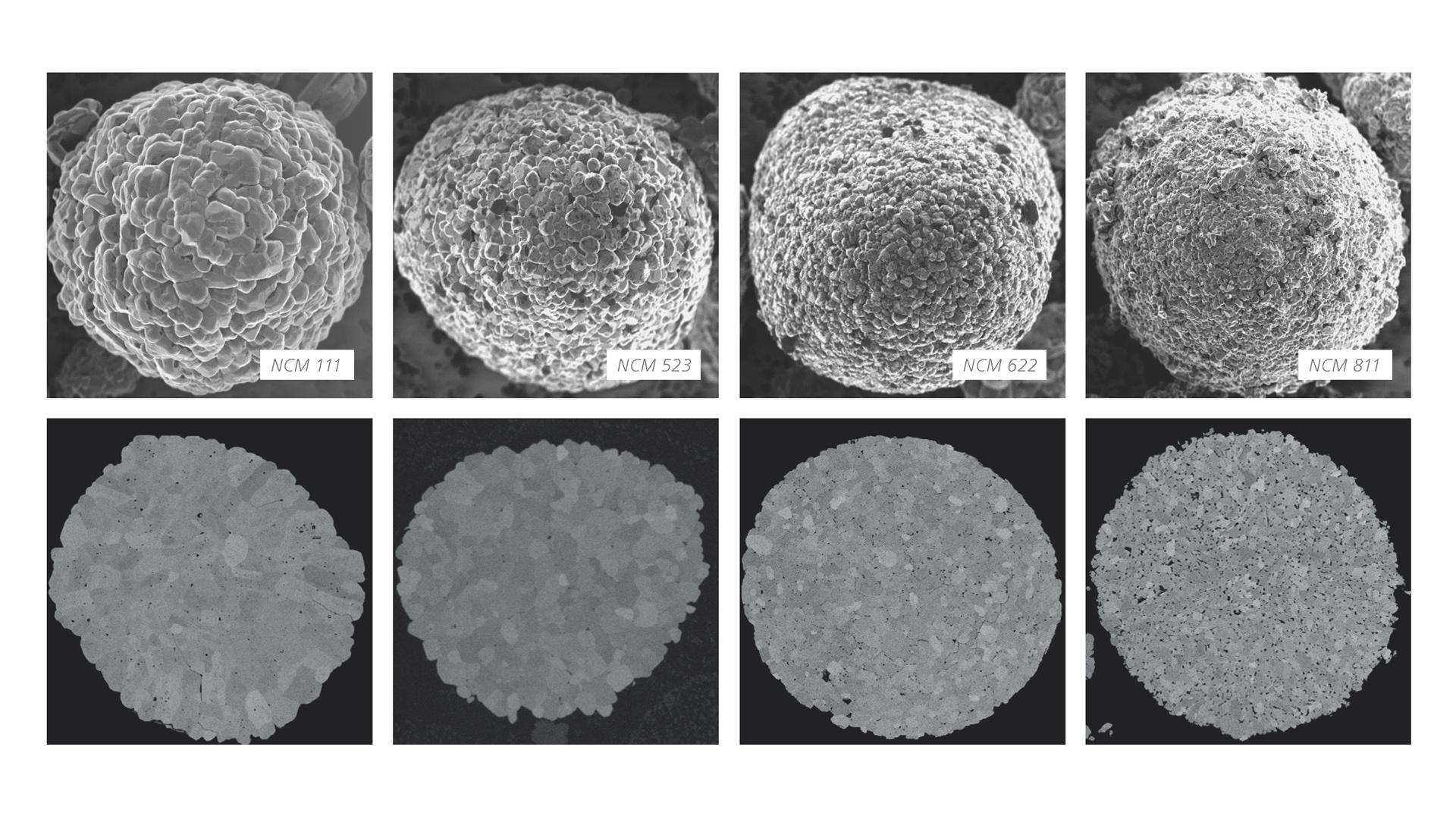
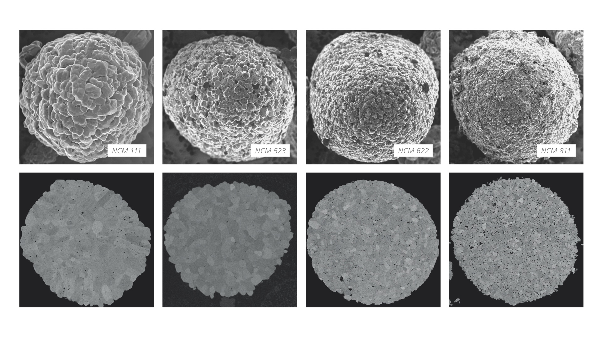
  • Surface, microstructure, and device characterization​
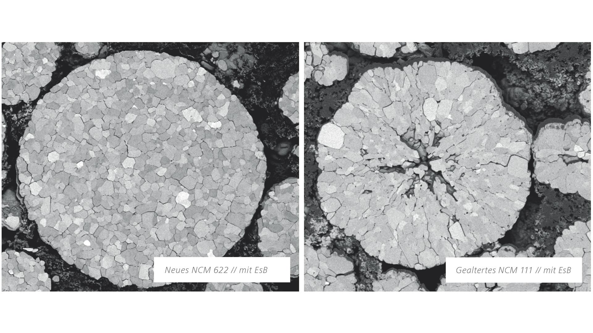
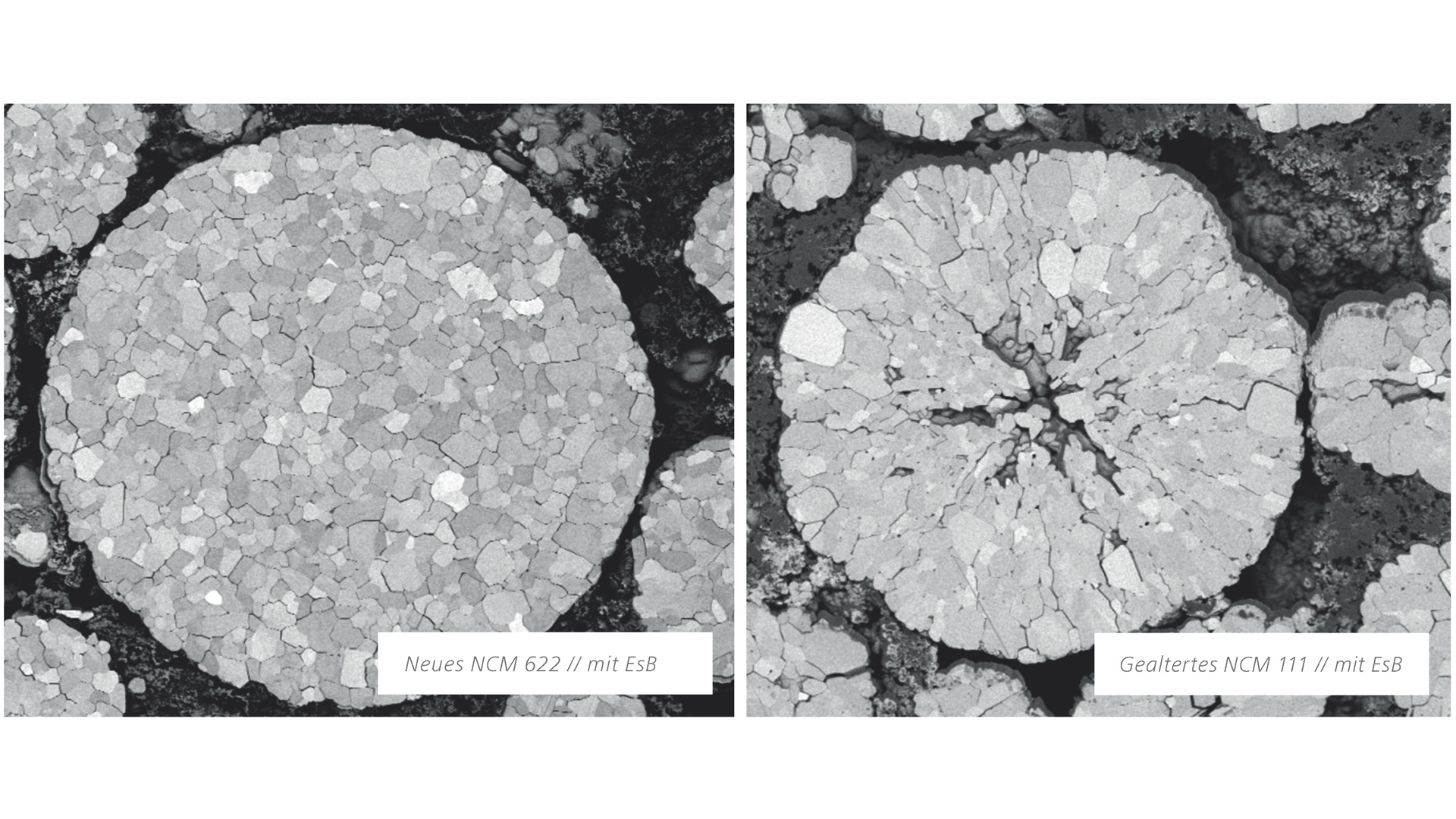
  • Compositional and phase distribution​
  • Impurity and inclusion determination​

Learn more in our videos about GeminiSEM

  • Heating and Tensile Experiments | In Situ for ZEISS FE-SEM​

    Watch the new workflow video and learn how to perform automated in situ heating and tensile experiments with In Situ Lab for ZEISS​
  • ZEISS GeminiSEM Family: Your FE-SEMs for Ultimate Imaging and Effortless Analytics​

    ZEISS GeminiSEM Family offers three new models to researchers of disciplines from materials to life sciences. Three unique designs for the Gemini electron optics and a large, flexible new chamber cover all your imaging and analytical needs.​

Imaging and material analysis of lithium-ion batteries

  • Cathode materials in the automotive industry​

    The performance of functional materials and advanced devices such as batteries, solar cells and fuel cells depends on the microstructure of the material used. In order for these material composites to deliver the desired performance, the interplay between many different materials must work.​

    The focus here is on the materials nickel, manganese and cobalt. This type of battery is called Li-NMC, LNMC, NMC or NCM. The designations NCM 111, 523 etc. indicate the respective composition ratio of nickel, cobalt and manganese. The example shows the cross-section of a lithium-ion battery with a cathode made of NCM 111. The charging and discharging of lithium-ion batteries leads to changes in the microstructure. Cracks occur, which increase the surface area of the SEI layer. This reduces the battery performance.​

  • Using an electron microscope, we can see that there are structural differences between the NCM variants when other production factors are fundamentally accounted for. When seen in cross section, the primary particles of 811 are much smaller than those of 532 or 111. This excellent material contrast of the sub-grain structure is visible only with a feature unique to ZEISS electron microscopes – the Energy Selective Backscatter (EsB) detector.​

    A better composition of the electrolytes can lead to less physical wear of the cathode materials. With better chemical processes, cathode materials with larger grain particles can be produced.​

  • Lithium-ion battery cell: EDX element distribution image​

    Cross section of full-stack lithium ion battery cell: EDS mapping (O, Al, F, Si, and C). It is possible to use energy dispersive spectroscopy (EDS) to confirm the elemental composition of objects under investigation in the microscope. ​

    This image confirms high levels of residual fluorine on the cathode side, as expected in an aged sample. Fluorine is found in the electrolyte and joins an SEI layer that increases with aging. The boehmite separator shows aluminum and oxygen signals, as expected. Carbon is used as a conductive agent in the binder. As the polymer of the separator is a hydrocarbon, this means carbon can be seen throughout the battery.​

  • Material analysis: Grain size analysis with AI segmentation

    Grain size and distribution are directly related to the material characteristics. Quantify the crystallographic structure of yourstructure of your materials according to international standards. You can characterize your samples using three evaluation methods:​

    • Planimetric method for the automatic reconstruction of grain boundaries​
    • Intercept method with a variety of different measuring grids for interactive detection and counting of grain boundary intersections​
    • Comparison method for manual image evaluation with comparison diagrams​
  • ZEISS ZEN Intellesis software uses machine learning algorithms and a pre-trained model to recognize the foreign phase and grain boundaries. One click and you can select the instance segmentation model and the class to be segmented.​

    The results view contains all images and results of the analysis performed. The original images are also shown. You can view all the results of the analysis in a clear table view as well as in a bar chart for the grain size distribution.​

Downloads

  • ZEISS SEM Brochure A4 EN PDF

    Pages: 19
    File size: 22 MB

Contact us​

Interested in exploring our products or services further? We're excited to offer you more details or a live demo, either remotely or in person.​

Do you need more information?

Get in touch with us. Our experts will get back to you.

Form is loading...

/ 4
Next Step:
  • Interest Inquiry
  • Personal Details
  • Company Details

If you want to have more information on data processing at ZEISS please refer to our data privacy notice.