![Analoge Mikrochips und Packaging-Systeme Analoge Mikrochips und Packaging-Systeme]({"xsmall":"https://www.zeiss.com/content/dam/rms/reference-master/applications/electronics-and-semiconductor/microscopy-solutions-for-semiconductor-and-electronics/analog-rf-power-mems-sensors-microscopy-solutions.jpg/_jcr_content/renditions/original.image_file.100.100.240,0,1680,1440.file/analog-rf-power-mems-sensors-microscopy-solutions.jpg","small":"https://www.zeiss.com/content/dam/rms/reference-master/applications/electronics-and-semiconductor/microscopy-solutions-for-semiconductor-and-electronics/analog-rf-power-mems-sensors-microscopy-solutions.jpg/_jcr_content/renditions/original.image_file.360.360.240,0,1680,1440.file/analog-rf-power-mems-sensors-microscopy-solutions.jpg","medium":"https://www.zeiss.com/content/dam/rms/reference-master/applications/electronics-and-semiconductor/microscopy-solutions-for-semiconductor-and-electronics/analog-rf-power-mems-sensors-microscopy-solutions.jpg/_jcr_content/renditions/original.image_file.768.768.240,0,1680,1440.file/analog-rf-power-mems-sensors-microscopy-solutions.jpg","large":"https://www.zeiss.com/content/dam/rms/reference-master/applications/electronics-and-semiconductor/microscopy-solutions-for-semiconductor-and-electronics/analog-rf-power-mems-sensors-microscopy-solutions.jpg/_jcr_content/renditions/original.image_file.1024.1024.240,0,1680,1440.file/analog-rf-power-mems-sensors-microscopy-solutions.jpg","xlarge":"https://www.zeiss.com/content/dam/rms/reference-master/applications/electronics-and-semiconductor/microscopy-solutions-for-semiconductor-and-electronics/analog-rf-power-mems-sensors-microscopy-solutions.jpg/_jcr_content/renditions/original.image_file.1280.1280.240,0,1680,1440.file/analog-rf-power-mems-sensors-microscopy-solutions.jpg","xxlarge":"https://www.zeiss.com/content/dam/rms/reference-master/applications/electronics-and-semiconductor/microscopy-solutions-for-semiconductor-and-electronics/analog-rf-power-mems-sensors-microscopy-solutions.jpg/_jcr_content/renditions/original.image_file.1440.1440.240,0,1680,1440.file/analog-rf-power-mems-sensors-microscopy-solutions.jpg","max":"https://www.zeiss.com/content/dam/rms/reference-master/applications/electronics-and-semiconductor/microscopy-solutions-for-semiconductor-and-electronics/analog-rf-power-mems-sensors-microscopy-solutions.jpg/_jcr_content/renditions/original.image_file.1440.1440.240,0,1680,1440.file/analog-rf-power-mems-sensors-microscopy-solutions.jpg"})
Erweiterte Analysen für komplexe neuartige Materialien und Strukturen
Kürzere Time-to-Market durch akkurate Fehleranalyse
Mobilfunk, das Internet der Dinge (IoT), Cloud Computing und die Elektrifizierung der Automobilindustrie erzeugen eine immense Nachfrage nach hochleistungsfähigen „More than Moore“-Halbleiterkomponenten, mit neuartigen Materialien und Prozessen, neuen Siliziumarchitekturen und Packaging-Technologien wie den mikroelektromechanischen Systemen (MEMS). Materialien mit direkter oder breiter Bandlücke wie Galliumarsenid (GaAs), Siliziumkarbid (SiC) und Galliumnitrid (GaN) stellen Hersteller von Geräten und Komponenten gleichermaßen vor neue Herausforderungen. Viele dieser Komponenten nutzen nach wie vor auch herkömmliche integrierte Schaltkreise (IC), was die Anforderungen an Herstellung und Packaging weiter erhöht.
Um den Entwicklungszyklus und die Time-to-Market dieser anspruchsvollen Bauteile zu beschleunigen, benötigen Hersteller modernste Analysetools, die komplexe Integrationen neuer Materialien und Fehlerursachen-Analysen unterstützen.
![IGBT-Querschnitt und EDX-Elementverteilungsbild IGBT-Querschnitt und EDX-Elementverteilungsbild]({"xsmall":"https://www.zeiss.com/content/dam/rms/reference-master/applications/electronics-and-semiconductor/microscopy-solutions-for-semiconductor-and-electronics/insulated-gate-bipolar-transistor-cross-section-and-edx-map-fib-sem.jpg/_jcr_content/renditions/original.image_file.100.100.0,0,1920,1920.file/insulated-gate-bipolar-transistor-cross-section-and-edx-map-fib-sem.jpg","small":"https://www.zeiss.com/content/dam/rms/reference-master/applications/electronics-and-semiconductor/microscopy-solutions-for-semiconductor-and-electronics/insulated-gate-bipolar-transistor-cross-section-and-edx-map-fib-sem.jpg/_jcr_content/renditions/original.image_file.360.360.0,0,1920,1920.file/insulated-gate-bipolar-transistor-cross-section-and-edx-map-fib-sem.jpg","medium":"https://www.zeiss.com/content/dam/rms/reference-master/applications/electronics-and-semiconductor/microscopy-solutions-for-semiconductor-and-electronics/insulated-gate-bipolar-transistor-cross-section-and-edx-map-fib-sem.jpg/_jcr_content/renditions/original.image_file.768.768.0,0,1920,1920.file/insulated-gate-bipolar-transistor-cross-section-and-edx-map-fib-sem.jpg","large":"https://www.zeiss.com/content/dam/rms/reference-master/applications/electronics-and-semiconductor/microscopy-solutions-for-semiconductor-and-electronics/insulated-gate-bipolar-transistor-cross-section-and-edx-map-fib-sem.jpg/_jcr_content/renditions/original.image_file.1024.1024.0,0,1920,1920.file/insulated-gate-bipolar-transistor-cross-section-and-edx-map-fib-sem.jpg","xlarge":"https://www.zeiss.com/content/dam/rms/reference-master/applications/electronics-and-semiconductor/microscopy-solutions-for-semiconductor-and-electronics/insulated-gate-bipolar-transistor-cross-section-and-edx-map-fib-sem.jpg/_jcr_content/renditions/original.image_file.1280.1280.0,0,1920,1920.file/insulated-gate-bipolar-transistor-cross-section-and-edx-map-fib-sem.jpg","xxlarge":"https://www.zeiss.com/content/dam/rms/reference-master/applications/electronics-and-semiconductor/microscopy-solutions-for-semiconductor-and-electronics/insulated-gate-bipolar-transistor-cross-section-and-edx-map-fib-sem.jpg/_jcr_content/renditions/original.image_file.1440.1440.0,0,1920,1920.file/insulated-gate-bipolar-transistor-cross-section-and-edx-map-fib-sem.jpg","max":"https://www.zeiss.com/content/dam/rms/reference-master/applications/electronics-and-semiconductor/microscopy-solutions-for-semiconductor-and-electronics/insulated-gate-bipolar-transistor-cross-section-and-edx-map-fib-sem.jpg/_jcr_content/renditions/original.image_file.1920.1920.0,0,1920,1920.file/insulated-gate-bipolar-transistor-cross-section-and-edx-map-fib-sem.jpg"})
Querschnitt und EDX eines IGBT
![IGBT-Querschnitt und EDX-Elementverteilungsbild IGBT-Querschnitt und EDX-Elementverteilungsbild]({"xsmall":"https://www.zeiss.com/content/dam/rms/reference-master/applications/electronics-and-semiconductor/microscopy-solutions-for-semiconductor-and-electronics/insulated-gate-bipolar-transistor-cross-section-and-edx-map-fib-sem.jpg/_jcr_content/renditions/original.image_file.100.100.file/insulated-gate-bipolar-transistor-cross-section-and-edx-map-fib-sem.jpg","small":"https://www.zeiss.com/content/dam/rms/reference-master/applications/electronics-and-semiconductor/microscopy-solutions-for-semiconductor-and-electronics/insulated-gate-bipolar-transistor-cross-section-and-edx-map-fib-sem.jpg/_jcr_content/renditions/original.image_file.360.360.file/insulated-gate-bipolar-transistor-cross-section-and-edx-map-fib-sem.jpg","medium":"https://www.zeiss.com/content/dam/rms/reference-master/applications/electronics-and-semiconductor/microscopy-solutions-for-semiconductor-and-electronics/insulated-gate-bipolar-transistor-cross-section-and-edx-map-fib-sem.jpg/_jcr_content/renditions/original.image_file.768.768.file/insulated-gate-bipolar-transistor-cross-section-and-edx-map-fib-sem.jpg","large":"https://www.zeiss.com/content/dam/rms/reference-master/applications/electronics-and-semiconductor/microscopy-solutions-for-semiconductor-and-electronics/insulated-gate-bipolar-transistor-cross-section-and-edx-map-fib-sem.jpg/_jcr_content/renditions/original.image_file.1024.1023.file/insulated-gate-bipolar-transistor-cross-section-and-edx-map-fib-sem.jpg","xlarge":"https://www.zeiss.com/content/dam/rms/reference-master/applications/electronics-and-semiconductor/microscopy-solutions-for-semiconductor-and-electronics/insulated-gate-bipolar-transistor-cross-section-and-edx-map-fib-sem.jpg/_jcr_content/renditions/original.image_file.1280.1279.file/insulated-gate-bipolar-transistor-cross-section-and-edx-map-fib-sem.jpg","xxlarge":"https://www.zeiss.com/content/dam/rms/reference-master/applications/electronics-and-semiconductor/microscopy-solutions-for-semiconductor-and-electronics/insulated-gate-bipolar-transistor-cross-section-and-edx-map-fib-sem.jpg/_jcr_content/renditions/original.image_file.1440.1439.file/insulated-gate-bipolar-transistor-cross-section-and-edx-map-fib-sem.jpg","max":"https://www.zeiss.com/content/dam/rms/reference-master/applications/electronics-and-semiconductor/microscopy-solutions-for-semiconductor-and-electronics/insulated-gate-bipolar-transistor-cross-section-and-edx-map-fib-sem.jpg/_jcr_content/renditions/original./insulated-gate-bipolar-transistor-cross-section-and-edx-map-fib-sem.jpg"})
Querschnitt und EDX eines IGBT
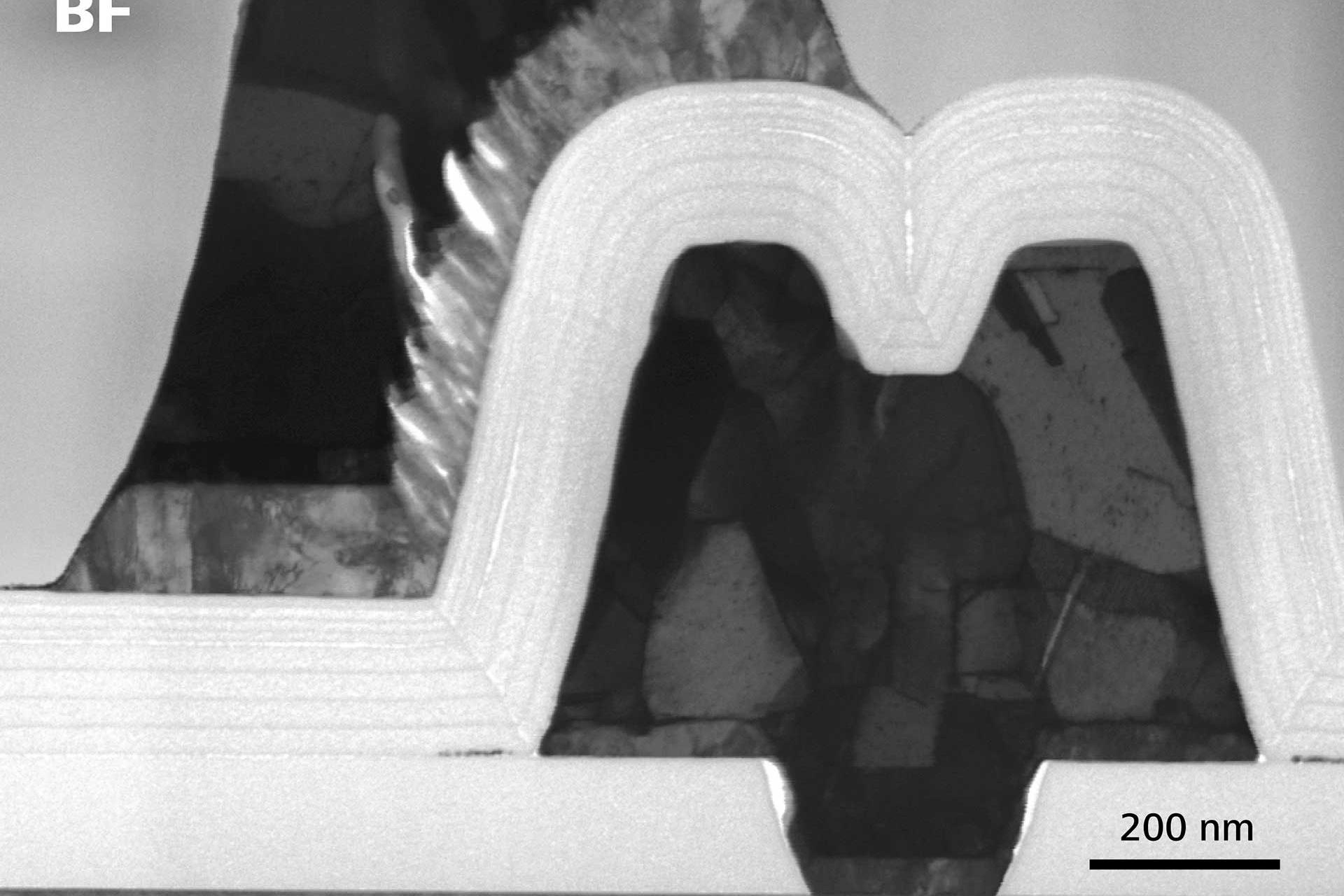
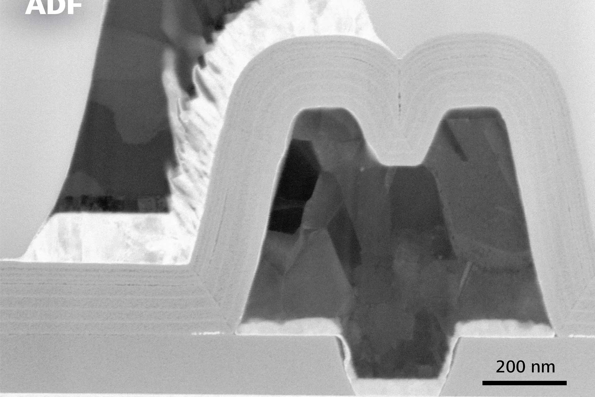
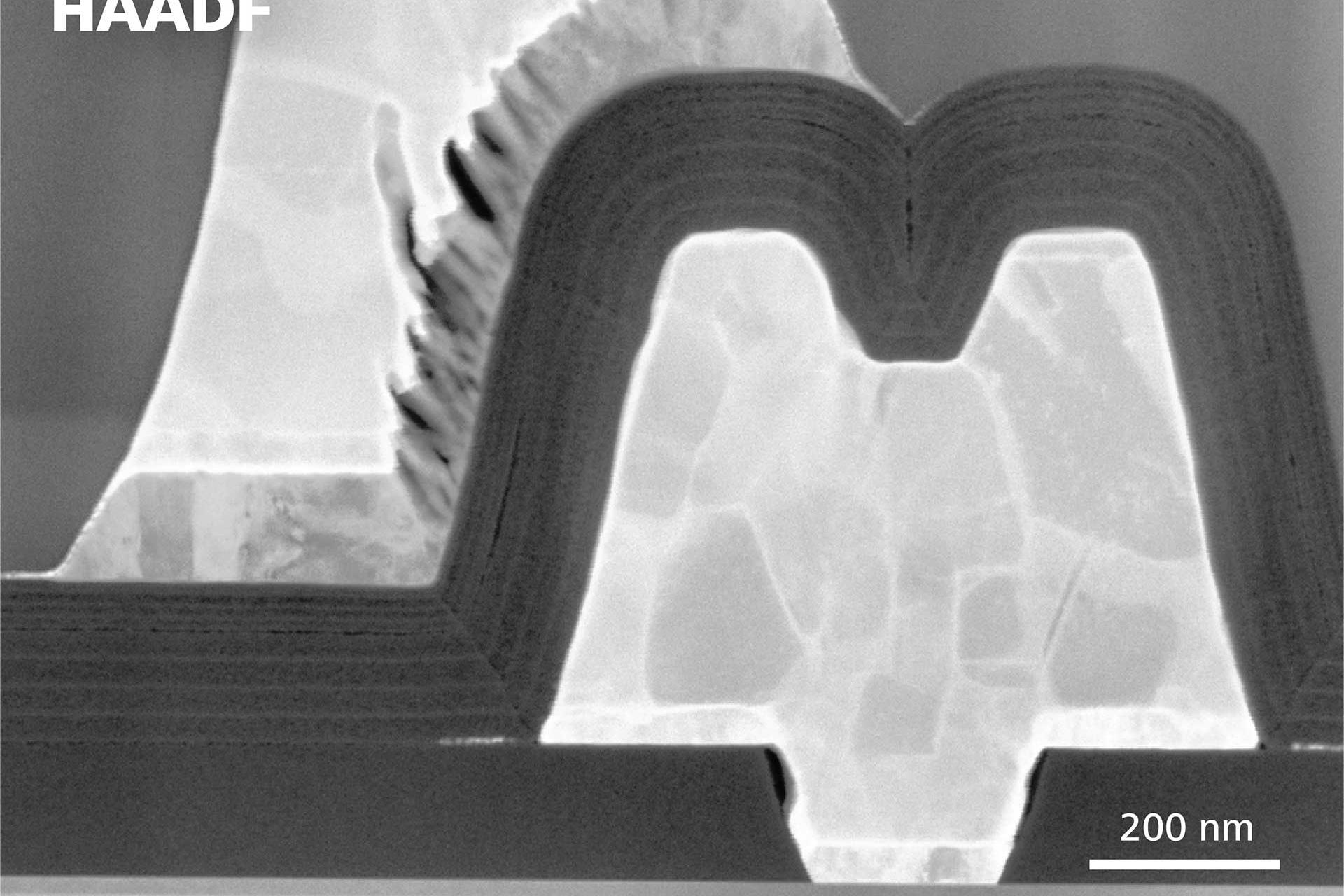
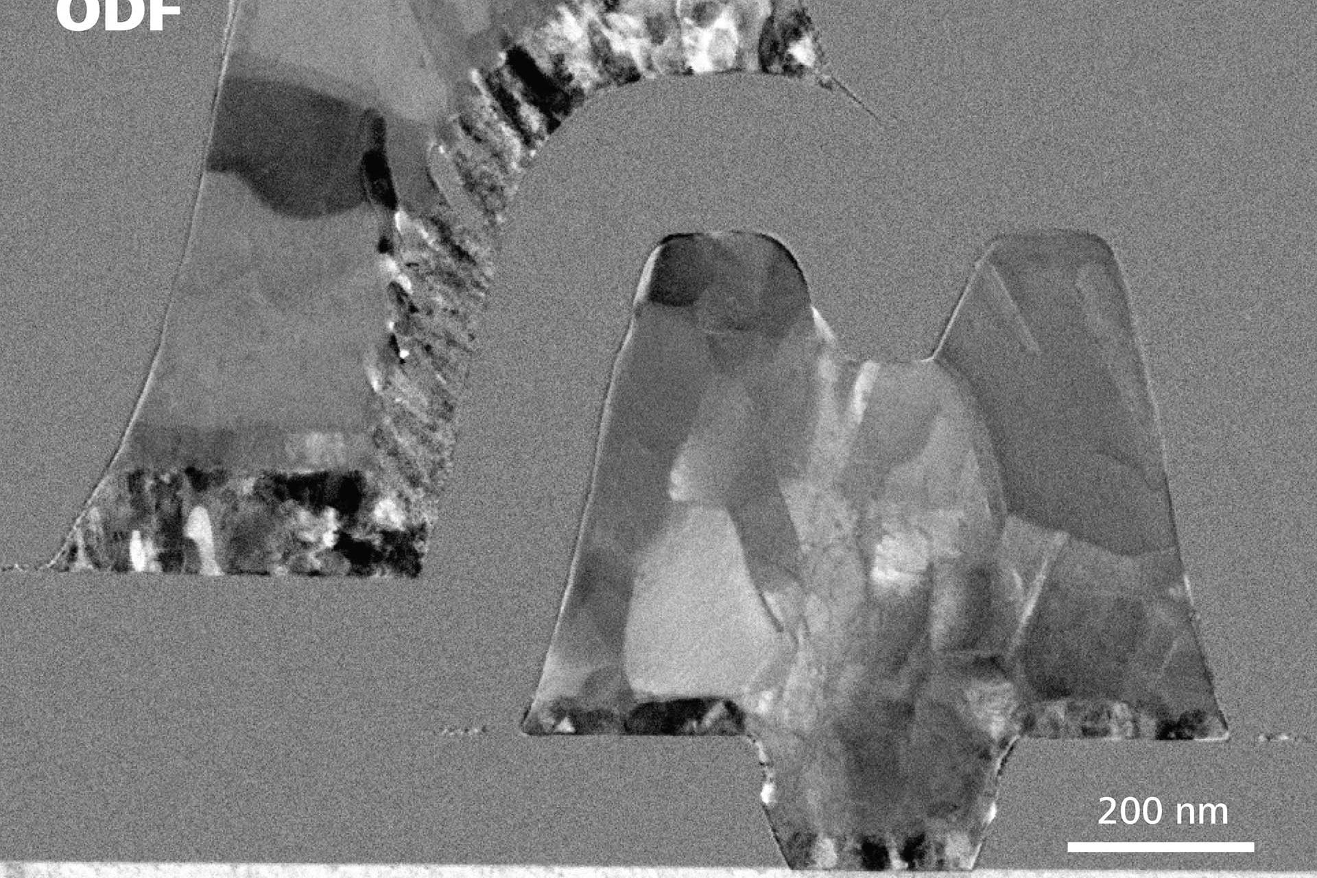
Untersuchung der Grenzschicht eines Gates in einem Bipolartransistor mit isolierter Steuerelektrode (Insulated Gate Bipolar Transistor, IGBT). Die gesamte Querschnitt- und EDX-Elementaranalyse wurde mit einem ZEISS Crossbeam 550 FIB-SEM durchgeführt. Das STEM-in-SEM-Bild (Hellfeld, 30 kV) einer Lamelle zeigt in Kombination mit dem EDX-Elementverteilungsbild in Crossbeam kristalline Si-Ausfällungen.
![SiC-MOSFET-Dotierungsprofil SiC-MOSFET-Dotierungsprofil]({"xsmall":"https://www.zeiss.com/content/dam/rms/reference-master/applications/electronics-and-semiconductor/microscopy-solutions-for-semiconductor-and-electronics/silicon-carbide-mosfet-dopant-profiling-fib-sem.jpg/_jcr_content/renditions/original.image_file.100.75.0,0,1917,1439.file/silicon-carbide-mosfet-dopant-profiling-fib-sem.jpg","small":"https://www.zeiss.com/content/dam/rms/reference-master/applications/electronics-and-semiconductor/microscopy-solutions-for-semiconductor-and-electronics/silicon-carbide-mosfet-dopant-profiling-fib-sem.jpg/_jcr_content/renditions/original.image_file.360.270.0,0,1917,1439.file/silicon-carbide-mosfet-dopant-profiling-fib-sem.jpg","medium":"https://www.zeiss.com/content/dam/rms/reference-master/applications/electronics-and-semiconductor/microscopy-solutions-for-semiconductor-and-electronics/silicon-carbide-mosfet-dopant-profiling-fib-sem.jpg/_jcr_content/renditions/original.image_file.768.576.0,0,1917,1439.file/silicon-carbide-mosfet-dopant-profiling-fib-sem.jpg","large":"https://www.zeiss.com/content/dam/rms/reference-master/applications/electronics-and-semiconductor/microscopy-solutions-for-semiconductor-and-electronics/silicon-carbide-mosfet-dopant-profiling-fib-sem.jpg/_jcr_content/renditions/original.image_file.1024.768.0,0,1917,1439.file/silicon-carbide-mosfet-dopant-profiling-fib-sem.jpg","xlarge":"https://www.zeiss.com/content/dam/rms/reference-master/applications/electronics-and-semiconductor/microscopy-solutions-for-semiconductor-and-electronics/silicon-carbide-mosfet-dopant-profiling-fib-sem.jpg/_jcr_content/renditions/original.image_file.1280.960.0,0,1917,1439.file/silicon-carbide-mosfet-dopant-profiling-fib-sem.jpg","xxlarge":"https://www.zeiss.com/content/dam/rms/reference-master/applications/electronics-and-semiconductor/microscopy-solutions-for-semiconductor-and-electronics/silicon-carbide-mosfet-dopant-profiling-fib-sem.jpg/_jcr_content/renditions/original.image_file.1440.1080.0,0,1917,1439.file/silicon-carbide-mosfet-dopant-profiling-fib-sem.jpg","max":"https://www.zeiss.com/content/dam/rms/reference-master/applications/electronics-and-semiconductor/microscopy-solutions-for-semiconductor-and-electronics/silicon-carbide-mosfet-dopant-profiling-fib-sem.jpg/_jcr_content/renditions/original.image_file.1917.1438.0,0,1917,1439.file/silicon-carbide-mosfet-dopant-profiling-fib-sem.jpg"})
Aufnahme des Dotierungsprofils eines SiC-MOFSET
![SiC-MOSFET-Dotierungsprofil SiC-MOSFET-Dotierungsprofil]({"xsmall":"https://www.zeiss.com/content/dam/rms/reference-master/applications/electronics-and-semiconductor/microscopy-solutions-for-semiconductor-and-electronics/silicon-carbide-mosfet-dopant-profiling-fib-sem.jpg/_jcr_content/renditions/original.image_file.100.75.file/silicon-carbide-mosfet-dopant-profiling-fib-sem.jpg","small":"https://www.zeiss.com/content/dam/rms/reference-master/applications/electronics-and-semiconductor/microscopy-solutions-for-semiconductor-and-electronics/silicon-carbide-mosfet-dopant-profiling-fib-sem.jpg/_jcr_content/renditions/original.image_file.360.270.file/silicon-carbide-mosfet-dopant-profiling-fib-sem.jpg","medium":"https://www.zeiss.com/content/dam/rms/reference-master/applications/electronics-and-semiconductor/microscopy-solutions-for-semiconductor-and-electronics/silicon-carbide-mosfet-dopant-profiling-fib-sem.jpg/_jcr_content/renditions/original.image_file.768.576.file/silicon-carbide-mosfet-dopant-profiling-fib-sem.jpg","large":"https://www.zeiss.com/content/dam/rms/reference-master/applications/electronics-and-semiconductor/microscopy-solutions-for-semiconductor-and-electronics/silicon-carbide-mosfet-dopant-profiling-fib-sem.jpg/_jcr_content/renditions/original.image_file.1024.768.file/silicon-carbide-mosfet-dopant-profiling-fib-sem.jpg","xlarge":"https://www.zeiss.com/content/dam/rms/reference-master/applications/electronics-and-semiconductor/microscopy-solutions-for-semiconductor-and-electronics/silicon-carbide-mosfet-dopant-profiling-fib-sem.jpg/_jcr_content/renditions/original.image_file.1280.960.file/silicon-carbide-mosfet-dopant-profiling-fib-sem.jpg","xxlarge":"https://www.zeiss.com/content/dam/rms/reference-master/applications/electronics-and-semiconductor/microscopy-solutions-for-semiconductor-and-electronics/silicon-carbide-mosfet-dopant-profiling-fib-sem.jpg/_jcr_content/renditions/original.image_file.1440.1080.file/silicon-carbide-mosfet-dopant-profiling-fib-sem.jpg","max":"https://www.zeiss.com/content/dam/rms/reference-master/applications/electronics-and-semiconductor/microscopy-solutions-for-semiconductor-and-electronics/silicon-carbide-mosfet-dopant-profiling-fib-sem.jpg/_jcr_content/renditions/original./silicon-carbide-mosfet-dopant-profiling-fib-sem.jpg"})
Aufnahme des Dotierungsprofils eines SiC-MOFSET
Gespaltenes SiC-MOSFET-Bauteil, aufgenommen bei 1,5 kV mit einem ZEISS Crossbeam FIB-SEM. Die Aufnahme hebt die unterschiedlich dotierten Bereiche hervor, die auf die unterschiedlichen Arbeitsfunktionen zurückgehen. Das dunkle Band, das sich unterhalb und auf beide Seiten des Gates erstreckt, zeigt die n+-Diffusion. Die helle Zone zeigt den Bereich des p-Typ-Körpers. Diese Technik gibt Aufschluss über den Zustand und die Lokalisation der Sperrschicht.
3D‑Röntgen-Imaging der Hauptplatine eines Smartphones im Nanobereich
![3D-Bild eines Beschleunigungssensors (MEMS) 3D-Bild eines Beschleunigungssensors (MEMS)]({"xsmall":"https://www.zeiss.com/content/dam/rms/reference-master/applications/electronics-and-semiconductor/microscopy-solutions-for-semiconductor-and-electronics/smartphone-gyroscope-mems-3d-xrm.jpg/_jcr_content/renditions/original.image_file.100.100.file/smartphone-gyroscope-mems-3d-xrm.jpg","small":"https://www.zeiss.com/content/dam/rms/reference-master/applications/electronics-and-semiconductor/microscopy-solutions-for-semiconductor-and-electronics/smartphone-gyroscope-mems-3d-xrm.jpg/_jcr_content/renditions/original.image_file.360.360.file/smartphone-gyroscope-mems-3d-xrm.jpg","medium":"https://www.zeiss.com/content/dam/rms/reference-master/applications/electronics-and-semiconductor/microscopy-solutions-for-semiconductor-and-electronics/smartphone-gyroscope-mems-3d-xrm.jpg/_jcr_content/renditions/original.image_file.768.768.file/smartphone-gyroscope-mems-3d-xrm.jpg","large":"https://www.zeiss.com/content/dam/rms/reference-master/applications/electronics-and-semiconductor/microscopy-solutions-for-semiconductor-and-electronics/smartphone-gyroscope-mems-3d-xrm.jpg/_jcr_content/renditions/original.image_file.1024.1024.file/smartphone-gyroscope-mems-3d-xrm.jpg","xlarge":"https://www.zeiss.com/content/dam/rms/reference-master/applications/electronics-and-semiconductor/microscopy-solutions-for-semiconductor-and-electronics/smartphone-gyroscope-mems-3d-xrm.jpg/_jcr_content/renditions/original.image_file.1280.1280.file/smartphone-gyroscope-mems-3d-xrm.jpg","xxlarge":"https://www.zeiss.com/content/dam/rms/reference-master/applications/electronics-and-semiconductor/microscopy-solutions-for-semiconductor-and-electronics/smartphone-gyroscope-mems-3d-xrm.jpg/_jcr_content/renditions/original.image_file.1440.1440.file/smartphone-gyroscope-mems-3d-xrm.jpg","max":"https://www.zeiss.com/content/dam/rms/reference-master/applications/electronics-and-semiconductor/microscopy-solutions-for-semiconductor-and-electronics/smartphone-gyroscope-mems-3d-xrm.jpg/_jcr_content/renditions/original./smartphone-gyroscope-mems-3d-xrm.jpg"})
3D‑Analyse des Gyroskops/Beschleunigungssensors eines Smartphones
3D‑Röntgen-Rekonstruktion der Silizium-Mikrokamm-Strukturen, Auflösung: 1 µm/Voxel.
Aufgenommen mit ZEISS Xradia Versa-Röntgenmikroskop
![Draufsicht auf den MEMS-Beschleunigungssensor, mit schmaler Kammstruktur Draufsicht auf den MEMS-Beschleunigungssensor, mit schmaler Kammstruktur]({"xsmall":"https://www.zeiss.com/content/dam/rms/reference-master/applications/electronics-and-semiconductor/microscopy-solutions-for-semiconductor-and-electronics/smartphone-gyroscope-mems-fine-comb-fins-3d-xrm-plan-view.jpg/_jcr_content/renditions/original.image_file.100.100.file/smartphone-gyroscope-mems-fine-comb-fins-3d-xrm-plan-view.jpg","small":"https://www.zeiss.com/content/dam/rms/reference-master/applications/electronics-and-semiconductor/microscopy-solutions-for-semiconductor-and-electronics/smartphone-gyroscope-mems-fine-comb-fins-3d-xrm-plan-view.jpg/_jcr_content/renditions/original.image_file.360.360.file/smartphone-gyroscope-mems-fine-comb-fins-3d-xrm-plan-view.jpg","medium":"https://www.zeiss.com/content/dam/rms/reference-master/applications/electronics-and-semiconductor/microscopy-solutions-for-semiconductor-and-electronics/smartphone-gyroscope-mems-fine-comb-fins-3d-xrm-plan-view.jpg/_jcr_content/renditions/original.image_file.768.768.file/smartphone-gyroscope-mems-fine-comb-fins-3d-xrm-plan-view.jpg","large":"https://www.zeiss.com/content/dam/rms/reference-master/applications/electronics-and-semiconductor/microscopy-solutions-for-semiconductor-and-electronics/smartphone-gyroscope-mems-fine-comb-fins-3d-xrm-plan-view.jpg/_jcr_content/renditions/original.image_file.1024.1024.file/smartphone-gyroscope-mems-fine-comb-fins-3d-xrm-plan-view.jpg","xlarge":"https://www.zeiss.com/content/dam/rms/reference-master/applications/electronics-and-semiconductor/microscopy-solutions-for-semiconductor-and-electronics/smartphone-gyroscope-mems-fine-comb-fins-3d-xrm-plan-view.jpg/_jcr_content/renditions/original.image_file.1280.1280.file/smartphone-gyroscope-mems-fine-comb-fins-3d-xrm-plan-view.jpg","xxlarge":"https://www.zeiss.com/content/dam/rms/reference-master/applications/electronics-and-semiconductor/microscopy-solutions-for-semiconductor-and-electronics/smartphone-gyroscope-mems-fine-comb-fins-3d-xrm-plan-view.jpg/_jcr_content/renditions/original.image_file.1440.1440.file/smartphone-gyroscope-mems-fine-comb-fins-3d-xrm-plan-view.jpg","max":"https://www.zeiss.com/content/dam/rms/reference-master/applications/electronics-and-semiconductor/microscopy-solutions-for-semiconductor-and-electronics/smartphone-gyroscope-mems-fine-comb-fins-3d-xrm-plan-view.jpg/_jcr_content/renditions/original./smartphone-gyroscope-mems-fine-comb-fins-3d-xrm-plan-view.jpg"})
Hochauflösende Aufnahme feiner Kammzähne
Virtuelle Draufsicht derselben Analyse mit feinen Kammzähnen, Auflösung: 0,3 µm/Voxel.
Aufgenommen mit ZEISS Xradia Versa-Röntgenmikroskop
![MEMS-Beschleunigungssensor, Querschnitt der schmalen Kammstruktur MEMS-Beschleunigungssensor, Querschnitt der schmalen Kammstruktur]({"xsmall":"https://www.zeiss.com/content/dam/rms/reference-master/applications/electronics-and-semiconductor/microscopy-solutions-for-semiconductor-and-electronics/smartphone-gyroscope-mems-fine-comb-fins-3d-xrm-cross-section.jpg/_jcr_content/renditions/original.image_file.100.100.file/smartphone-gyroscope-mems-fine-comb-fins-3d-xrm-cross-section.jpg","small":"https://www.zeiss.com/content/dam/rms/reference-master/applications/electronics-and-semiconductor/microscopy-solutions-for-semiconductor-and-electronics/smartphone-gyroscope-mems-fine-comb-fins-3d-xrm-cross-section.jpg/_jcr_content/renditions/original.image_file.360.360.file/smartphone-gyroscope-mems-fine-comb-fins-3d-xrm-cross-section.jpg","medium":"https://www.zeiss.com/content/dam/rms/reference-master/applications/electronics-and-semiconductor/microscopy-solutions-for-semiconductor-and-electronics/smartphone-gyroscope-mems-fine-comb-fins-3d-xrm-cross-section.jpg/_jcr_content/renditions/original.image_file.768.768.file/smartphone-gyroscope-mems-fine-comb-fins-3d-xrm-cross-section.jpg","large":"https://www.zeiss.com/content/dam/rms/reference-master/applications/electronics-and-semiconductor/microscopy-solutions-for-semiconductor-and-electronics/smartphone-gyroscope-mems-fine-comb-fins-3d-xrm-cross-section.jpg/_jcr_content/renditions/original.image_file.1024.1024.file/smartphone-gyroscope-mems-fine-comb-fins-3d-xrm-cross-section.jpg","xlarge":"https://www.zeiss.com/content/dam/rms/reference-master/applications/electronics-and-semiconductor/microscopy-solutions-for-semiconductor-and-electronics/smartphone-gyroscope-mems-fine-comb-fins-3d-xrm-cross-section.jpg/_jcr_content/renditions/original.image_file.1280.1280.file/smartphone-gyroscope-mems-fine-comb-fins-3d-xrm-cross-section.jpg","xxlarge":"https://www.zeiss.com/content/dam/rms/reference-master/applications/electronics-and-semiconductor/microscopy-solutions-for-semiconductor-and-electronics/smartphone-gyroscope-mems-fine-comb-fins-3d-xrm-cross-section.jpg/_jcr_content/renditions/original.image_file.1440.1440.file/smartphone-gyroscope-mems-fine-comb-fins-3d-xrm-cross-section.jpg","max":"https://www.zeiss.com/content/dam/rms/reference-master/applications/electronics-and-semiconductor/microscopy-solutions-for-semiconductor-and-electronics/smartphone-gyroscope-mems-fine-comb-fins-3d-xrm-cross-section.jpg/_jcr_content/renditions/original./smartphone-gyroscope-mems-fine-comb-fins-3d-xrm-cross-section.jpg"})
Virtueller Schnitt der Kammzähne
Virtueller Querschnitt derselben Probe mit detaillierter Abbildung der 2,1 µm feinen Kammzähne, Auflösung: 0,3 µm/Voxel.
Aufgenommen mit ZEISS Xradia Versa-Röntgenmikroskop
Zerstörungsfreie Analysen für System, Packaging und Schaltungen
![3D‑Röntgenbild eines Smartphones 3D‑Röntgenbild eines Smartphones]({"xsmall":"https://www.zeiss.com/content/dam/rms/reference-master/applications/electronics-and-semiconductor/microscopy-solutions-for-semiconductor-and-electronics/smartphone-3d-xrm-image.jpg/_jcr_content/renditions/original.image_file.100.100.240,0,1680,1440.file/smartphone-3d-xrm-image.jpg","small":"https://www.zeiss.com/content/dam/rms/reference-master/applications/electronics-and-semiconductor/microscopy-solutions-for-semiconductor-and-electronics/smartphone-3d-xrm-image.jpg/_jcr_content/renditions/original.image_file.360.360.240,0,1680,1440.file/smartphone-3d-xrm-image.jpg","medium":"https://www.zeiss.com/content/dam/rms/reference-master/applications/electronics-and-semiconductor/microscopy-solutions-for-semiconductor-and-electronics/smartphone-3d-xrm-image.jpg/_jcr_content/renditions/original.image_file.768.768.240,0,1680,1440.file/smartphone-3d-xrm-image.jpg","large":"https://www.zeiss.com/content/dam/rms/reference-master/applications/electronics-and-semiconductor/microscopy-solutions-for-semiconductor-and-electronics/smartphone-3d-xrm-image.jpg/_jcr_content/renditions/original.image_file.1024.1024.240,0,1680,1440.file/smartphone-3d-xrm-image.jpg","xlarge":"https://www.zeiss.com/content/dam/rms/reference-master/applications/electronics-and-semiconductor/microscopy-solutions-for-semiconductor-and-electronics/smartphone-3d-xrm-image.jpg/_jcr_content/renditions/original.image_file.1280.1280.240,0,1680,1440.file/smartphone-3d-xrm-image.jpg","xxlarge":"https://www.zeiss.com/content/dam/rms/reference-master/applications/electronics-and-semiconductor/microscopy-solutions-for-semiconductor-and-electronics/smartphone-3d-xrm-image.jpg/_jcr_content/renditions/original.image_file.1440.1440.240,0,1680,1440.file/smartphone-3d-xrm-image.jpg","max":"https://www.zeiss.com/content/dam/rms/reference-master/applications/electronics-and-semiconductor/microscopy-solutions-for-semiconductor-and-electronics/smartphone-3d-xrm-image.jpg/_jcr_content/renditions/original.image_file.1440.1440.240,0,1680,1440.file/smartphone-3d-xrm-image.jpg"})
Smartphone
![3D‑Röntgenbild eines Smartphones 3D‑Röntgenbild eines Smartphones]({"xsmall":"https://www.zeiss.com/content/dam/rms/reference-master/applications/electronics-and-semiconductor/microscopy-solutions-for-semiconductor-and-electronics/smartphone-3d-xrm-image.jpg/_jcr_content/renditions/original.image_file.100.75.file/smartphone-3d-xrm-image.jpg","small":"https://www.zeiss.com/content/dam/rms/reference-master/applications/electronics-and-semiconductor/microscopy-solutions-for-semiconductor-and-electronics/smartphone-3d-xrm-image.jpg/_jcr_content/renditions/original.image_file.360.270.file/smartphone-3d-xrm-image.jpg","medium":"https://www.zeiss.com/content/dam/rms/reference-master/applications/electronics-and-semiconductor/microscopy-solutions-for-semiconductor-and-electronics/smartphone-3d-xrm-image.jpg/_jcr_content/renditions/original.image_file.768.576.file/smartphone-3d-xrm-image.jpg","large":"https://www.zeiss.com/content/dam/rms/reference-master/applications/electronics-and-semiconductor/microscopy-solutions-for-semiconductor-and-electronics/smartphone-3d-xrm-image.jpg/_jcr_content/renditions/original.image_file.1024.768.file/smartphone-3d-xrm-image.jpg","xlarge":"https://www.zeiss.com/content/dam/rms/reference-master/applications/electronics-and-semiconductor/microscopy-solutions-for-semiconductor-and-electronics/smartphone-3d-xrm-image.jpg/_jcr_content/renditions/original.image_file.1280.960.file/smartphone-3d-xrm-image.jpg","xxlarge":"https://www.zeiss.com/content/dam/rms/reference-master/applications/electronics-and-semiconductor/microscopy-solutions-for-semiconductor-and-electronics/smartphone-3d-xrm-image.jpg/_jcr_content/renditions/original.image_file.1440.1080.file/smartphone-3d-xrm-image.jpg","max":"https://www.zeiss.com/content/dam/rms/reference-master/applications/electronics-and-semiconductor/microscopy-solutions-for-semiconductor-and-electronics/smartphone-3d-xrm-image.jpg/_jcr_content/renditions/original./smartphone-3d-xrm-image.jpg"})
Smartphone
3D‑Röntgenabbildung eines kompletten Smartphones, Auflösung: 50 µm/Voxel.
Aufgenommen mit ZEISS Xradia Context microCT
![PMIC‑Package, virtuelle Draufsicht PMIC‑Package, virtuelle Draufsicht]({"xsmall":"https://www.zeiss.com/content/dam/rms/reference-master/applications/electronics-and-semiconductor/microscopy-solutions-for-semiconductor-and-electronics/smartphone-power-management-ic-package-3d-xrm-plan-view.jpg/_jcr_content/renditions/original.image_file.100.100.482,0,1921,1439.file/smartphone-power-management-ic-package-3d-xrm-plan-view.jpg","small":"https://www.zeiss.com/content/dam/rms/reference-master/applications/electronics-and-semiconductor/microscopy-solutions-for-semiconductor-and-electronics/smartphone-power-management-ic-package-3d-xrm-plan-view.jpg/_jcr_content/renditions/original.image_file.360.360.482,0,1921,1439.file/smartphone-power-management-ic-package-3d-xrm-plan-view.jpg","medium":"https://www.zeiss.com/content/dam/rms/reference-master/applications/electronics-and-semiconductor/microscopy-solutions-for-semiconductor-and-electronics/smartphone-power-management-ic-package-3d-xrm-plan-view.jpg/_jcr_content/renditions/original.image_file.768.768.482,0,1921,1439.file/smartphone-power-management-ic-package-3d-xrm-plan-view.jpg","large":"https://www.zeiss.com/content/dam/rms/reference-master/applications/electronics-and-semiconductor/microscopy-solutions-for-semiconductor-and-electronics/smartphone-power-management-ic-package-3d-xrm-plan-view.jpg/_jcr_content/renditions/original.image_file.1024.1024.482,0,1921,1439.file/smartphone-power-management-ic-package-3d-xrm-plan-view.jpg","xlarge":"https://www.zeiss.com/content/dam/rms/reference-master/applications/electronics-and-semiconductor/microscopy-solutions-for-semiconductor-and-electronics/smartphone-power-management-ic-package-3d-xrm-plan-view.jpg/_jcr_content/renditions/original.image_file.1280.1280.482,0,1921,1439.file/smartphone-power-management-ic-package-3d-xrm-plan-view.jpg","xxlarge":"https://www.zeiss.com/content/dam/rms/reference-master/applications/electronics-and-semiconductor/microscopy-solutions-for-semiconductor-and-electronics/smartphone-power-management-ic-package-3d-xrm-plan-view.jpg/_jcr_content/renditions/original.image_file.1439.1439.482,0,1921,1439.file/smartphone-power-management-ic-package-3d-xrm-plan-view.jpg","max":"https://www.zeiss.com/content/dam/rms/reference-master/applications/electronics-and-semiconductor/microscopy-solutions-for-semiconductor-and-electronics/smartphone-power-management-ic-package-3d-xrm-plan-view.jpg/_jcr_content/renditions/original.image_file.1439.1439.482,0,1921,1439.file/smartphone-power-management-ic-package-3d-xrm-plan-view.jpg"})
Power Management IC Package
![PMIC‑Package, virtuelle Draufsicht PMIC‑Package, virtuelle Draufsicht]({"xsmall":"https://www.zeiss.com/content/dam/rms/reference-master/applications/electronics-and-semiconductor/microscopy-solutions-for-semiconductor-and-electronics/smartphone-power-management-ic-package-3d-xrm-plan-view.jpg/_jcr_content/renditions/original.image_file.100.75.file/smartphone-power-management-ic-package-3d-xrm-plan-view.jpg","small":"https://www.zeiss.com/content/dam/rms/reference-master/applications/electronics-and-semiconductor/microscopy-solutions-for-semiconductor-and-electronics/smartphone-power-management-ic-package-3d-xrm-plan-view.jpg/_jcr_content/renditions/original.image_file.360.270.file/smartphone-power-management-ic-package-3d-xrm-plan-view.jpg","medium":"https://www.zeiss.com/content/dam/rms/reference-master/applications/electronics-and-semiconductor/microscopy-solutions-for-semiconductor-and-electronics/smartphone-power-management-ic-package-3d-xrm-plan-view.jpg/_jcr_content/renditions/original.image_file.768.576.file/smartphone-power-management-ic-package-3d-xrm-plan-view.jpg","large":"https://www.zeiss.com/content/dam/rms/reference-master/applications/electronics-and-semiconductor/microscopy-solutions-for-semiconductor-and-electronics/smartphone-power-management-ic-package-3d-xrm-plan-view.jpg/_jcr_content/renditions/original.image_file.1024.768.file/smartphone-power-management-ic-package-3d-xrm-plan-view.jpg","xlarge":"https://www.zeiss.com/content/dam/rms/reference-master/applications/electronics-and-semiconductor/microscopy-solutions-for-semiconductor-and-electronics/smartphone-power-management-ic-package-3d-xrm-plan-view.jpg/_jcr_content/renditions/original.image_file.1280.960.file/smartphone-power-management-ic-package-3d-xrm-plan-view.jpg","xxlarge":"https://www.zeiss.com/content/dam/rms/reference-master/applications/electronics-and-semiconductor/microscopy-solutions-for-semiconductor-and-electronics/smartphone-power-management-ic-package-3d-xrm-plan-view.jpg/_jcr_content/renditions/original.image_file.1440.1080.file/smartphone-power-management-ic-package-3d-xrm-plan-view.jpg","max":"https://www.zeiss.com/content/dam/rms/reference-master/applications/electronics-and-semiconductor/microscopy-solutions-for-semiconductor-and-electronics/smartphone-power-management-ic-package-3d-xrm-plan-view.jpg/_jcr_content/renditions/original./smartphone-power-management-ic-package-3d-xrm-plan-view.jpg"})
Power Management IC Package
Virtuelle Draufsicht eines Power Management Integrated Circuit Package (PMIC), Auflösung: 11 µm/Voxel.
Aufgenommen mit ZEISS Xradia Context microCT
![Querschnitt der PMIC‑Package-Schaltungen Querschnitt der PMIC‑Package-Schaltungen]({"xsmall":"https://www.zeiss.com/content/dam/rms/reference-master/applications/electronics-and-semiconductor/microscopy-solutions-for-semiconductor-and-electronics/smartphone-power-management-ic-interconnects-3d-xrm-cross-section.jpg/_jcr_content/renditions/original.image_file.100.100.482,0,1921,1439.file/smartphone-power-management-ic-interconnects-3d-xrm-cross-section.jpg","small":"https://www.zeiss.com/content/dam/rms/reference-master/applications/electronics-and-semiconductor/microscopy-solutions-for-semiconductor-and-electronics/smartphone-power-management-ic-interconnects-3d-xrm-cross-section.jpg/_jcr_content/renditions/original.image_file.360.360.482,0,1921,1439.file/smartphone-power-management-ic-interconnects-3d-xrm-cross-section.jpg","medium":"https://www.zeiss.com/content/dam/rms/reference-master/applications/electronics-and-semiconductor/microscopy-solutions-for-semiconductor-and-electronics/smartphone-power-management-ic-interconnects-3d-xrm-cross-section.jpg/_jcr_content/renditions/original.image_file.768.768.482,0,1921,1439.file/smartphone-power-management-ic-interconnects-3d-xrm-cross-section.jpg","large":"https://www.zeiss.com/content/dam/rms/reference-master/applications/electronics-and-semiconductor/microscopy-solutions-for-semiconductor-and-electronics/smartphone-power-management-ic-interconnects-3d-xrm-cross-section.jpg/_jcr_content/renditions/original.image_file.1024.1024.482,0,1921,1439.file/smartphone-power-management-ic-interconnects-3d-xrm-cross-section.jpg","xlarge":"https://www.zeiss.com/content/dam/rms/reference-master/applications/electronics-and-semiconductor/microscopy-solutions-for-semiconductor-and-electronics/smartphone-power-management-ic-interconnects-3d-xrm-cross-section.jpg/_jcr_content/renditions/original.image_file.1280.1280.482,0,1921,1439.file/smartphone-power-management-ic-interconnects-3d-xrm-cross-section.jpg","xxlarge":"https://www.zeiss.com/content/dam/rms/reference-master/applications/electronics-and-semiconductor/microscopy-solutions-for-semiconductor-and-electronics/smartphone-power-management-ic-interconnects-3d-xrm-cross-section.jpg/_jcr_content/renditions/original.image_file.1439.1439.482,0,1921,1439.file/smartphone-power-management-ic-interconnects-3d-xrm-cross-section.jpg","max":"https://www.zeiss.com/content/dam/rms/reference-master/applications/electronics-and-semiconductor/microscopy-solutions-for-semiconductor-and-electronics/smartphone-power-management-ic-interconnects-3d-xrm-cross-section.jpg/_jcr_content/renditions/original.image_file.1439.1439.482,0,1921,1439.file/smartphone-power-management-ic-interconnects-3d-xrm-cross-section.jpg"})
PMIC-Schaltungen
![Querschnitt der PMIC‑Package-Schaltungen Querschnitt der PMIC‑Package-Schaltungen]({"xsmall":"https://www.zeiss.com/content/dam/rms/reference-master/applications/electronics-and-semiconductor/microscopy-solutions-for-semiconductor-and-electronics/smartphone-power-management-ic-interconnects-3d-xrm-cross-section.jpg/_jcr_content/renditions/original.image_file.100.75.file/smartphone-power-management-ic-interconnects-3d-xrm-cross-section.jpg","small":"https://www.zeiss.com/content/dam/rms/reference-master/applications/electronics-and-semiconductor/microscopy-solutions-for-semiconductor-and-electronics/smartphone-power-management-ic-interconnects-3d-xrm-cross-section.jpg/_jcr_content/renditions/original.image_file.360.270.file/smartphone-power-management-ic-interconnects-3d-xrm-cross-section.jpg","medium":"https://www.zeiss.com/content/dam/rms/reference-master/applications/electronics-and-semiconductor/microscopy-solutions-for-semiconductor-and-electronics/smartphone-power-management-ic-interconnects-3d-xrm-cross-section.jpg/_jcr_content/renditions/original.image_file.768.576.file/smartphone-power-management-ic-interconnects-3d-xrm-cross-section.jpg","large":"https://www.zeiss.com/content/dam/rms/reference-master/applications/electronics-and-semiconductor/microscopy-solutions-for-semiconductor-and-electronics/smartphone-power-management-ic-interconnects-3d-xrm-cross-section.jpg/_jcr_content/renditions/original.image_file.1024.768.file/smartphone-power-management-ic-interconnects-3d-xrm-cross-section.jpg","xlarge":"https://www.zeiss.com/content/dam/rms/reference-master/applications/electronics-and-semiconductor/microscopy-solutions-for-semiconductor-and-electronics/smartphone-power-management-ic-interconnects-3d-xrm-cross-section.jpg/_jcr_content/renditions/original.image_file.1280.960.file/smartphone-power-management-ic-interconnects-3d-xrm-cross-section.jpg","xxlarge":"https://www.zeiss.com/content/dam/rms/reference-master/applications/electronics-and-semiconductor/microscopy-solutions-for-semiconductor-and-electronics/smartphone-power-management-ic-interconnects-3d-xrm-cross-section.jpg/_jcr_content/renditions/original.image_file.1440.1080.file/smartphone-power-management-ic-interconnects-3d-xrm-cross-section.jpg","max":"https://www.zeiss.com/content/dam/rms/reference-master/applications/electronics-and-semiconductor/microscopy-solutions-for-semiconductor-and-electronics/smartphone-power-management-ic-interconnects-3d-xrm-cross-section.jpg/_jcr_content/renditions/original./smartphone-power-management-ic-interconnects-3d-xrm-cross-section.jpg"})
Querschnitt der PMIC-Schaltungen
Virtueller Querschnitt der Lotbumps und Vias des PMIC, Auflösung: 2,1 µm/Voxel.
Aufgenommen mit der einzigartigen „Resolution at a Distance“ des ZEISS Xradia Versa-Röntgenmikroskops
EBAC eines analogen Chips
Untersuchung eines digitalen Zählchips mit einer Nanosonde im GeminiSEM bei 20 kV. Die EBAC-Abbildung (Elektronenstrahl getriggerter Absorptionsstrom-Kontrast oder Widerstandskontrast) enthält Informationen zu den Verbindungen der Verdrahtung unter der Oberfläche und den verborgenen p‑n-Übergängen.