

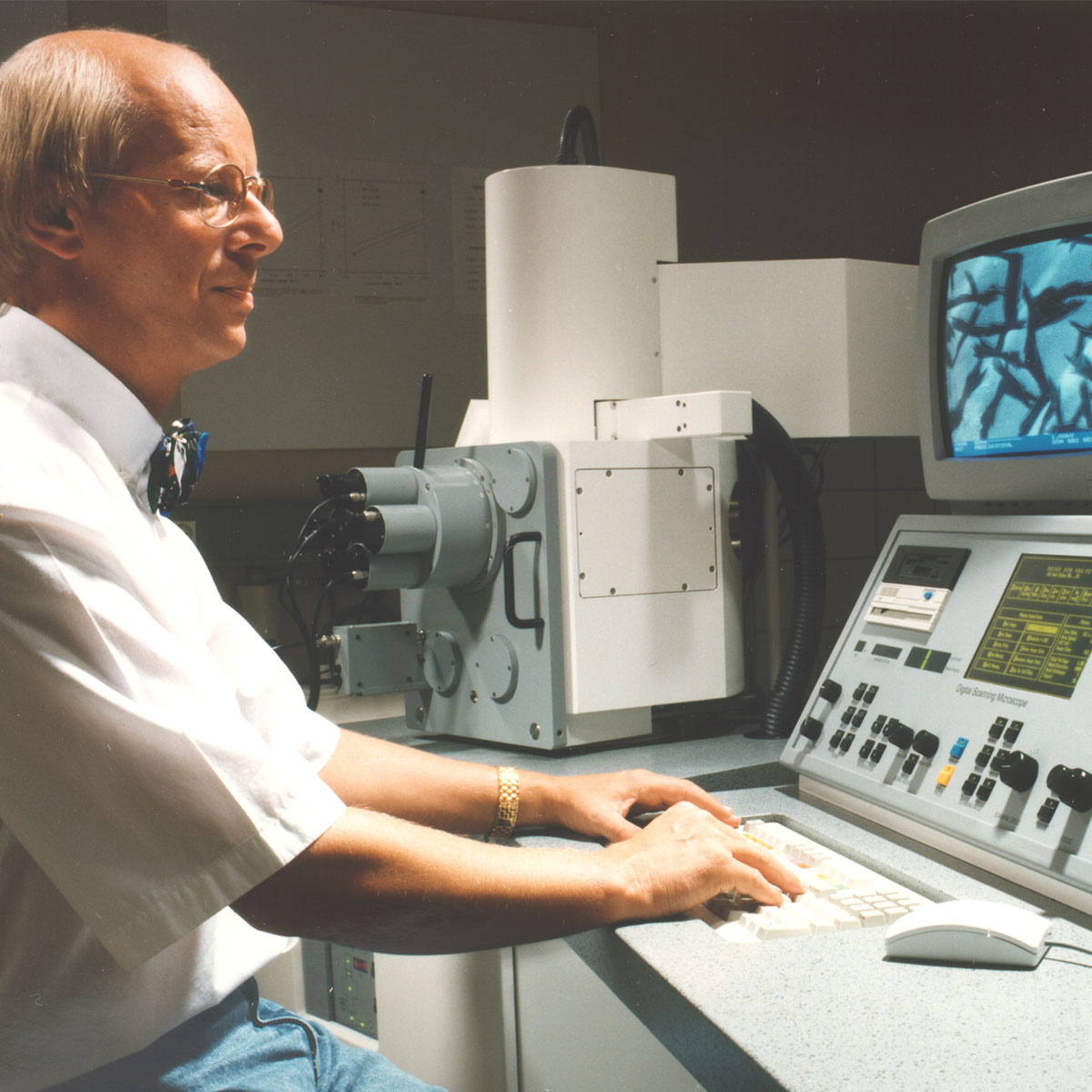
Testimonial
Dr. Mario Hentschel
Head of Cleanroom and Nanostructuring Facilities, first user of GeminiSEM 560
"We are dealing with micro- and nanostructures for optical sensing. Consequently, it is important to characterize devices on a nanometer scale. These applications require a large flexibility of the electron microscope. ZEISS GeminiSEM 560 is offering us an astonishing degree of freedom and flexibility. We obtain highest quality images even from very challenging samples, such as highly insulating polymers, showing minimal effects due to charging. The GeminiSEM 560 will thus definitely be an enabling technology for our research which we feel that this instrument can provide it in a very flexible way."


Testimonial
Dr. Theresa Magorian Friedlmeier
Senior Scientist Group Lead - Analysis and Simulation · Zentrum für Sonnenenergie- und Wasserstoff-Forschung Baden-Württemberg (ZSW)
"Microscopy is necessary for us to evaluate our layered systems. While the optical and electrical measurements provide us with the most relevant information about the solar cell function, we require materials analysis to relate the results to the processing. Since our layers are very thin, we use electron microscopy to determine the layer thicknesses in a cross-section image, either by cleaving or by FIB. The microstructure in the top view or cross-section provides us with information about grain size and roughness, as well as uniformity."
Testimonial
Kennedy Nguyen
The Imaging and Microscopy Facility (IMF) Manager at the University of California Merced
"As a core facility we have various instruments being shared by the entire university. Each lab has specific users with research that involves the SEM. Usually I help in the initial phases of their research and once they’re comfortable on their own, they operate the tool themselves. (This instrument) [,the GeminiSEM,] is nice because it’s one of the easiest SEMs to use, in my opinion."


TESTIMONIAL
Dr. Gong Ming
Deputy director, Lab of mechanical & materials science, University of science & technology, China
Dr. Gong Ming is using ZEISS GeminiSEM to serve more than 50 major projects of the National Natural Science Foundation, National Outstanding Youth Science Fund projects, National Key research and development programs.


TESTIMONIAL
Dr. Keyongsu Jeon
Senior Researcher Daegu Technopark, Technical Infrastructure Support Division Nanotechnology Processing Center, Korea
Dr. Keyongsu Jeon is currently researching various types of samples, such as nano-materials/components, ceramics, metals, polymers, bio or semiconductors, from diverse customers (both industries and academics).


TESTIMONIAL
Dr. Liuwen Chang
Professor, Department of Materials and Optoelectronic Science, National Sun Yat-sen University, Taiwan
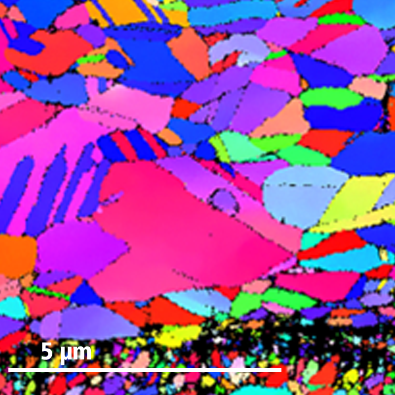
Dr. Chang, who researches electro-epitaxy of metals and compound semiconductors, uses SEM-based techniques such as EBSD, ECP, and ECCI to provide microstructural information of the epilayers in a non-destructive manner.


TESTIMONIAL
Dr. Jae Kim
Senior Researcher Ulsan Technopark, Fine Chemical & Material Technology Support Division, Korea
Dr. Jae Kim is currently researching the characterization of materials using scanning electron microscopy. He is particularly focused on the imaging of 3D printing-related polymeric materials, metal powders, and composites.


TESTIMONIAL
Dr. Satyam Suwas
Professor & Chair, Department of Materials Engineering, IISC, Bangalore
Dr. Satyam Suawas is currently researching deformed and annealed metals and alloys.


TESTIMONIAL
Dr. Savitha Purakkat
National Nanofabrication Centre, Centre for Nanoscience and Engineering, Indian Institute of Science, India
Dr. Savitha is currently researching dielectric film like, Al2O3, sub 50nm feature imaging.
Discover How Gemini Optics
has evolved
1 of 9
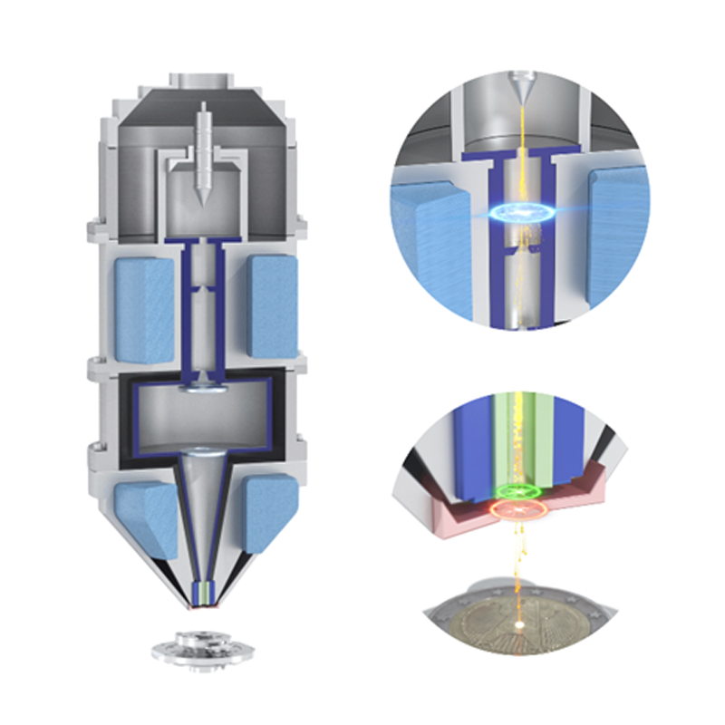
ZEISS GeminiSEM stands for effortless imaging with sub-nanometer resolution. These FE-SEMs (field emission scanning electron microscope) combine excellence in imaging and analytics. Innovations in electron optics and a new chamber design let you benefit from better image quality, usability and flexibility. Take sub-nanometer images below 1 kV without an immersion lens. Discover how Gemini optics has improved and evolved over time.
-
1993
Gemini 1 |
First FESEM With GEMINI OpticsThe combination of magnetic and electrostatic lens (Gemini optic lens) opens access to the world of low kV imaging. Photoresist and ceramic samples can be imaged uncoated without charging effects at high resolution with the DSM 982 Gemini.

-
2003
First Backscatter Detection (BSD)
at Low kVThe EsB detector is enabling in-column backscatter detection for the first time. The unique energy filtering properties are used to enhance the material contrast. Even nanocomposites can be analyzed with good material contrast with a small interaction volume.
Conventional diode detectors were not able to work below 5 kV, but the in-column EsB can provide this.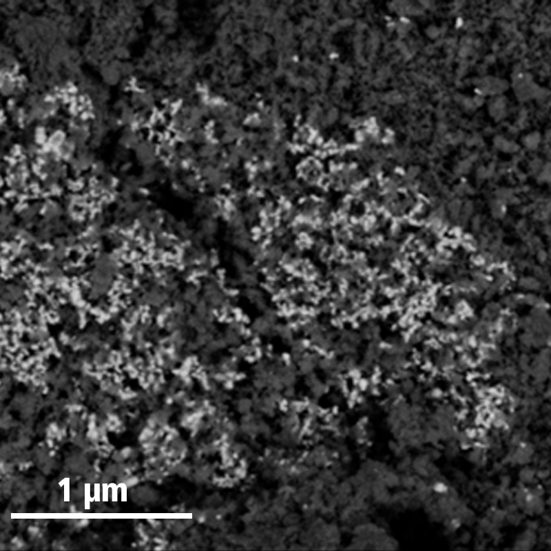
-
2004
Introduction of Sweet Spot Imaging
Cazaux and Grillon are publishing results showing the influence of the working distance for selective contrast imaging with the Gemini objective lens.
Sweet spot imaging means systematically varying the SEM accelerating voltage and working distance for optimum image quality.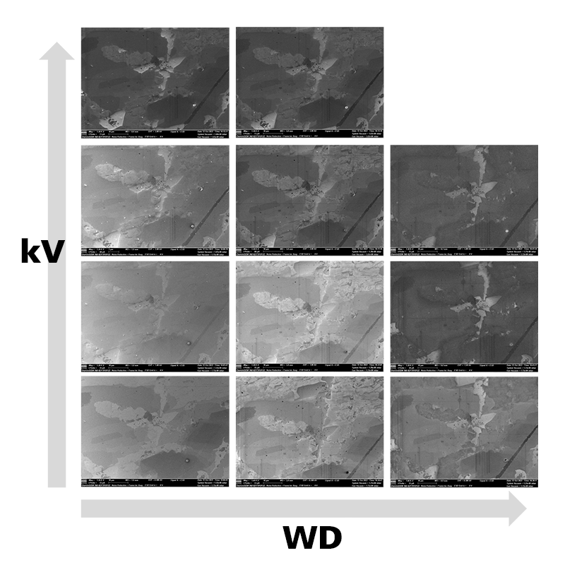
-
2009
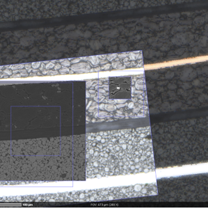
Correlative or Multi-Modal Microscopy
Correlative microscopy enables relocating regions of interest (ROI) in specimens in an electron microscope, which were previously identified in a light microscope and vice versa. The entire process takes only a few seconds. This opens up totally new dimensions in microscopy e.g., identification of ROIs with light microscopy and subsequent analytics in the SEM.
-
2010
Gemini 2 |
Double CondenserThe upper condenser sets the beam current, the lower condenser accounts for optimum resolution by optimizing the aperture angle, enabling high resolution at all beam currents. For a larger depth of field, the system can be switched to a different imaging mode and the convergence angle will be decreased.
-
2015
GeminiSEM with Nano-twin Lens
and NanoVPThe Nanotwin objective introduces a new lens design with lower aberration coefficients. It is optimized for ultra high resolution at low kV.
-
2018
Machine Learning for Microscopy
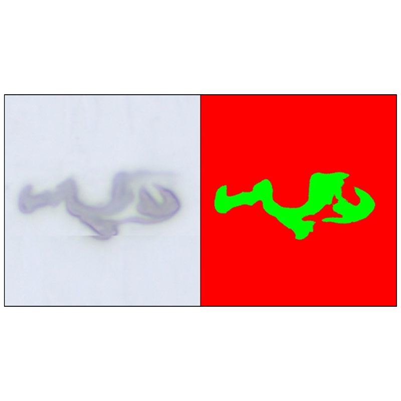
Zeiss ZEN Intellesis produces powerful machine learning segmentation of multidimensional images. It enables image segmentation and object classification without the need to code a single line.
-
2020
Gemini 3 |
Introduction of Smart AutopilotWith the Smart Autopilot, part of the new electron optical engine, Gemini 3 is able to ensure the highest possible resolution at each acceleration voltage.
-
2023
Gemini Optics Is Turning 30 Years 🎉
What an anniversary! Scroll further down to explore which microscopes use the technology, to which extend and last but not least, how the technology that we celebrate today works.
⬇️


What Makes the Difference?
Find out, which microscopes are using Gemini optics and what their advantages are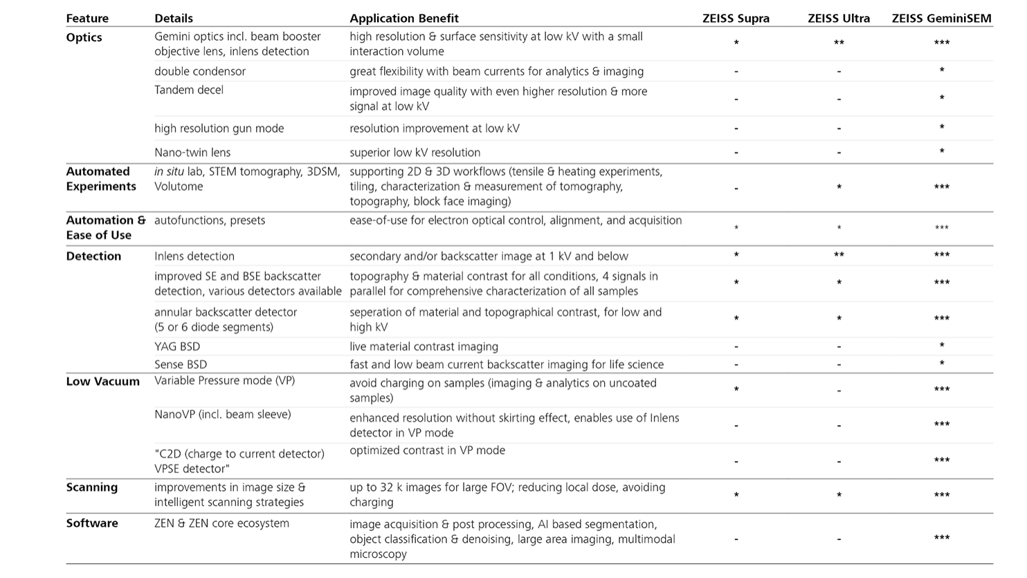


Click on the circle markers on the image to open the information box with more details.
Discover Gemini Optics


One Poster for Each Decade
Receive three posters about Gemini optics


Register here to receive a poster for each decade of Gemini optics
The first 1000 Registrants* can look forward to a free printed version sent via mailRegister here to receive a digital version of the Gemini optics posters.
As a special celebration gift for this anniversary, we will distribut printed versions to the first 1000 registrations via mail.
First come- first served, so be quick *