ZEISS Software Solutions

ZEISS @ Semicon Europa

Register for a free ticket

Starting soon
Ongoing Stay Tuned for next time
Ended Stay Tuned for next time
  • 00 years
  • 00 months
  • 00 days
  • 00 hours
  • 00 minutes
  • 00 seconds

Accelerating Digital Transformation and Innovation

ZEISS Solutions for Semiconductor Development, Manufacturing and Analysis

Digital technology is used everywhere in our modern economy. Higher performance and reliability from consumers’ interconnected devices drive the need for semiconductors with greater efficiency and miniaturization. Demand for high-performance, defect-free chips in multiple industries and consumer markets drives accelerated product development to supply a wide range of semiconductor and electronic products. Manufacturers must execute design-to-production cycles of highly complex devices with increasing speed. Intelligent workflows leveraging advanced microscopy solutions and software are required to rapidly resolve issues that critically affect manufacturing yield and device performance.
Register for a free trade show ticket and visit ZEISS at Semicon Europe 2024 in Hall B0 Booth XXX. Semicon will be held in parallel to Electronica, the ticket is valid for both events.

Please note:

  • Online registration in advance is required.
  • The online voucher link can only be redeemed once and is valid for one person at a time.
  • The tickets are only valid during the trade fair times.
  • Print out the ticket or show it mobile.
  • The ticket is valid for Semicon and Electronica.

Comprehensive Portfolio and Intelligent Workflows

Multi-Site lamella preparation in silicon using ZEN TEM Prep module in ZEN core. The array contains 7x6 1µm thick lamellas, aka chunks.

Microscopy Systems

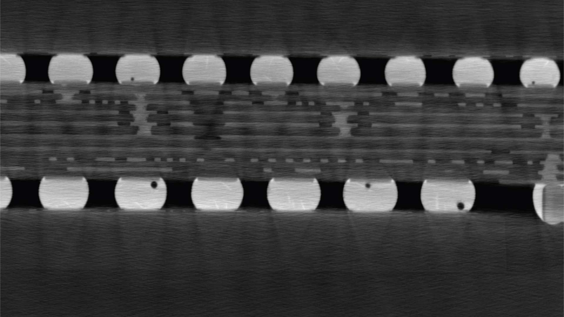
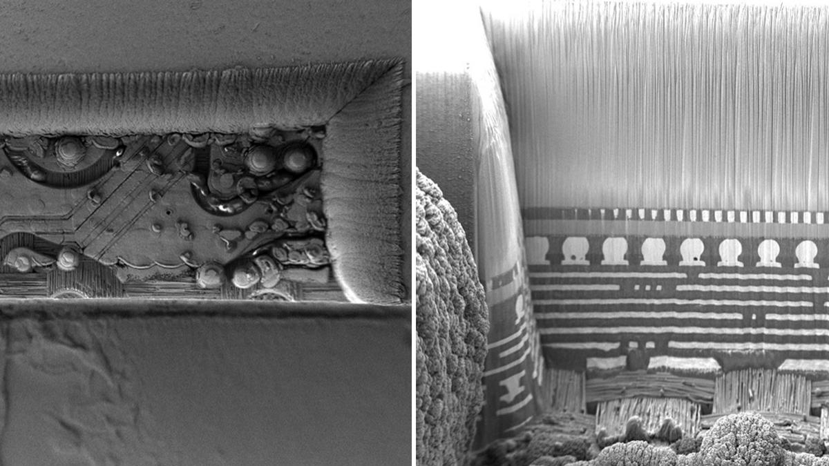
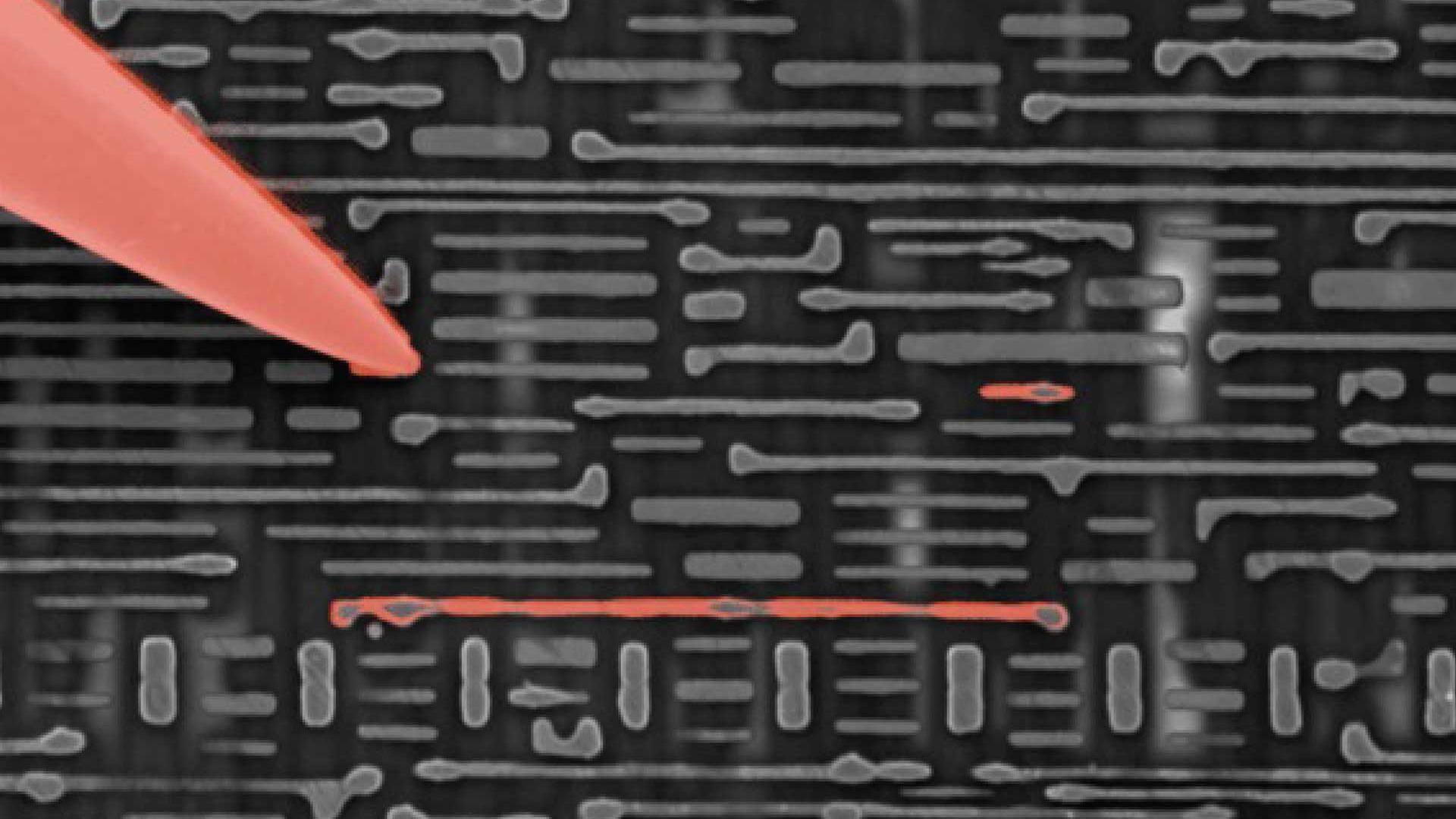
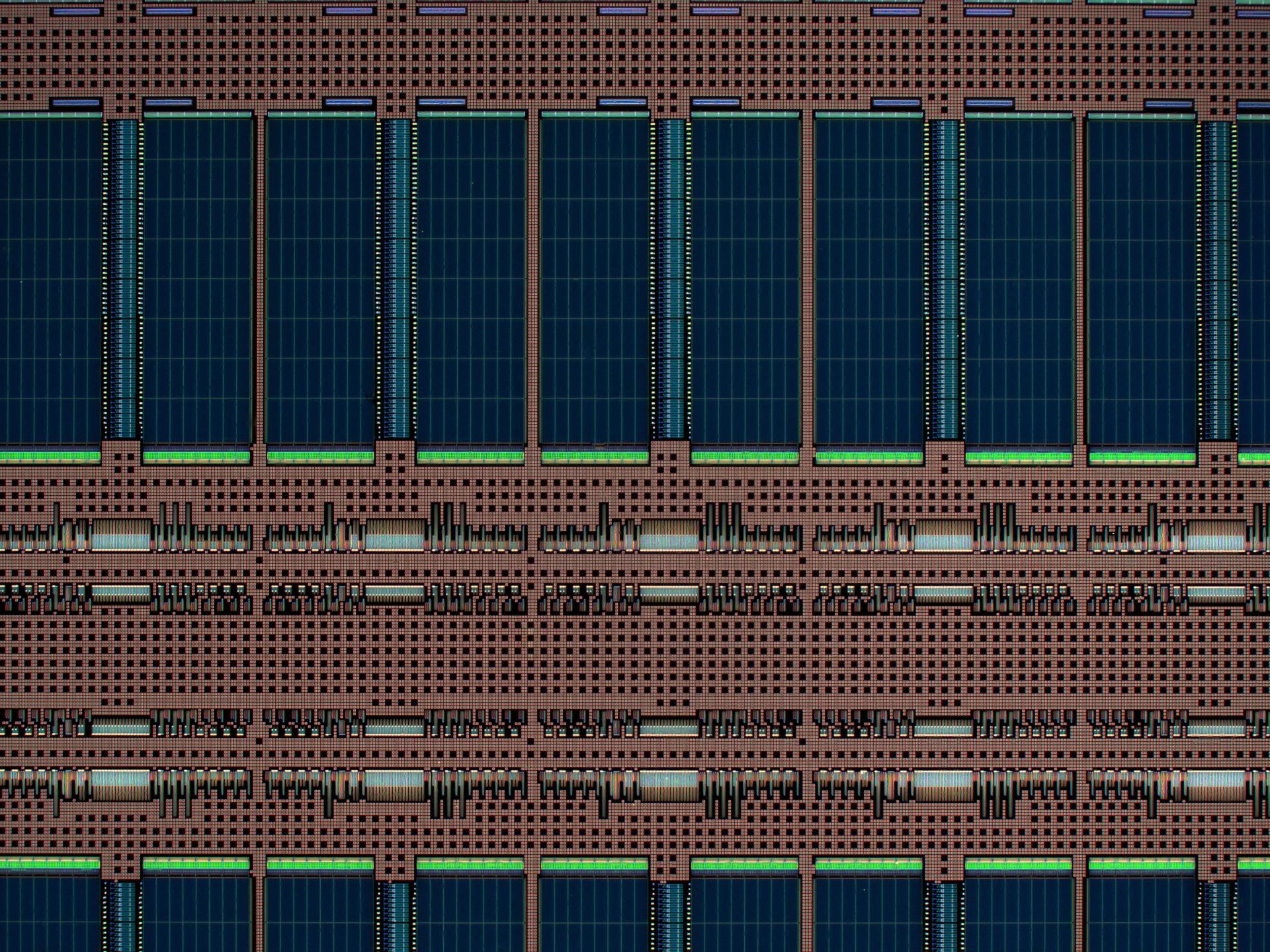
The Workflow for TEM Lamella Preparation. TEM lamella preparation is essential for almost any FIB-SEM user. ZEISS offers an automated workflow for site-specific preparation. The resulting lamellae are ideally suited for high resolution TEM and STEM imaging and analysis at atomic resolution. Navigate to the specimen’s ROI, extract your TEM lamella including ROI from your bulk sample, perform the bulk milling or trenching step, and finalize the workflow with lift-out and thinning where appropriate.

Axio Imager Vario

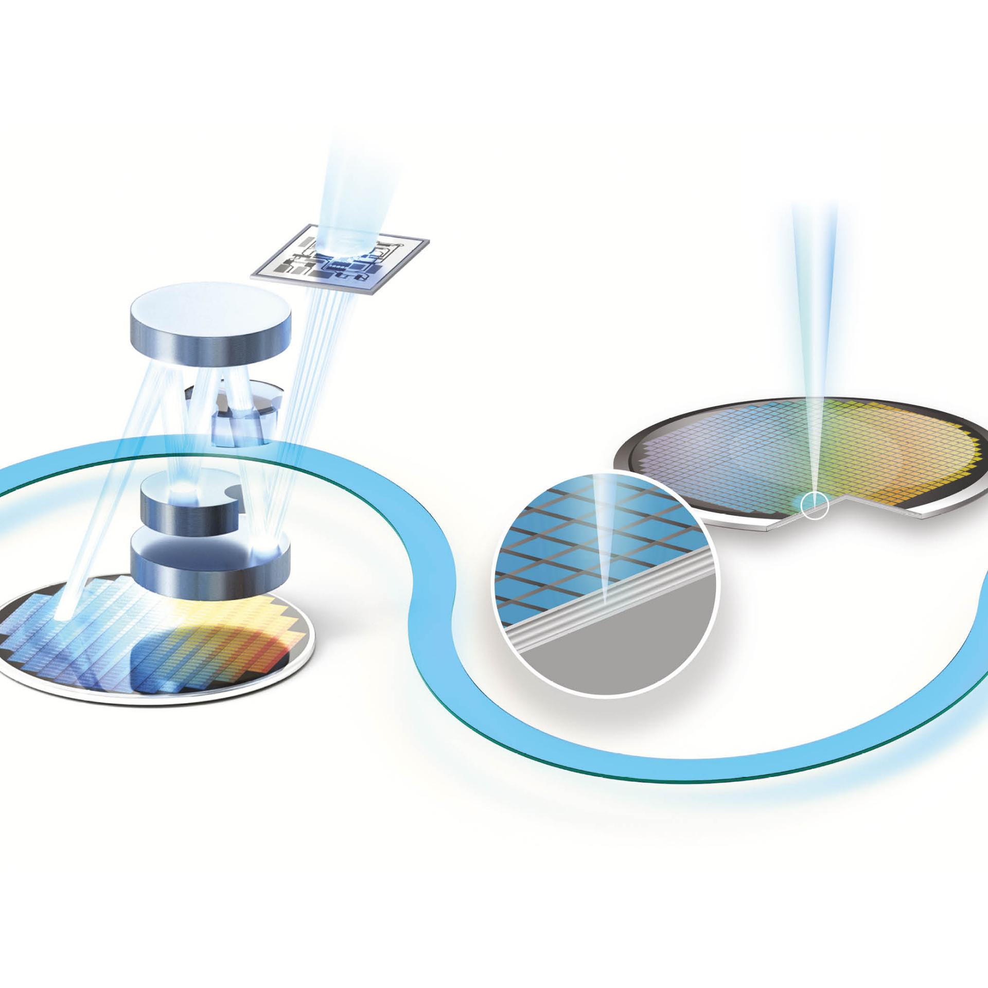
Analyze smallest MEMS sensors or an entire flat panel with ZEISS Axio Imager Vario. Its column design allows you to investigate extremely large specimens simultaneously offering high stability. Moreover, Axio Imager Vario is certified for use in clean rooms.

Individual software solutions

With our software engineering, we optimise and modernise infrastructures and environmental architectures in the cleanroom. We connect entire production chains, eliminate ineffective isolated solutions and anchor the possibility for cross-location platform architectures on a cloud basis. You benefit from higher quality, production reliability and more efficient use of resources.

Location

Semicon

Semicon Munich Messe München, Hall C2 535 81829 Munich Germany

Sign Up for Semicon Europa

Fill out the form & secure a free ticket

Form is loading...