![アナログマイクロチップとICパッケージ アナログマイクロチップとICパッケージ]({"xsmall":"https://www.zeiss.com/content/dam/rms/reference-master/applications/electronics-and-semiconductor/microscopy-solutions-for-semiconductor-and-electronics/analog-rf-power-mems-sensors-microscopy-solutions.jpg/_jcr_content/renditions/original.image_file.100.100.240,0,1680,1440.file/analog-rf-power-mems-sensors-microscopy-solutions.jpg","small":"https://www.zeiss.com/content/dam/rms/reference-master/applications/electronics-and-semiconductor/microscopy-solutions-for-semiconductor-and-electronics/analog-rf-power-mems-sensors-microscopy-solutions.jpg/_jcr_content/renditions/original.image_file.360.360.240,0,1680,1440.file/analog-rf-power-mems-sensors-microscopy-solutions.jpg","medium":"https://www.zeiss.com/content/dam/rms/reference-master/applications/electronics-and-semiconductor/microscopy-solutions-for-semiconductor-and-electronics/analog-rf-power-mems-sensors-microscopy-solutions.jpg/_jcr_content/renditions/original.image_file.768.768.240,0,1680,1440.file/analog-rf-power-mems-sensors-microscopy-solutions.jpg","large":"https://www.zeiss.com/content/dam/rms/reference-master/applications/electronics-and-semiconductor/microscopy-solutions-for-semiconductor-and-electronics/analog-rf-power-mems-sensors-microscopy-solutions.jpg/_jcr_content/renditions/original.image_file.1024.1024.240,0,1680,1440.file/analog-rf-power-mems-sensors-microscopy-solutions.jpg","xlarge":"https://www.zeiss.com/content/dam/rms/reference-master/applications/electronics-and-semiconductor/microscopy-solutions-for-semiconductor-and-electronics/analog-rf-power-mems-sensors-microscopy-solutions.jpg/_jcr_content/renditions/original.image_file.1280.1280.240,0,1680,1440.file/analog-rf-power-mems-sensors-microscopy-solutions.jpg","xxlarge":"https://www.zeiss.com/content/dam/rms/reference-master/applications/electronics-and-semiconductor/microscopy-solutions-for-semiconductor-and-electronics/analog-rf-power-mems-sensors-microscopy-solutions.jpg/_jcr_content/renditions/original.image_file.1440.1440.240,0,1680,1440.file/analog-rf-power-mems-sensors-microscopy-solutions.jpg","max":"https://www.zeiss.com/content/dam/rms/reference-master/applications/electronics-and-semiconductor/microscopy-solutions-for-semiconductor-and-electronics/analog-rf-power-mems-sensors-microscopy-solutions.jpg/_jcr_content/renditions/original.image_file.1440.1440.240,0,1680,1440.file/analog-rf-power-mems-sensors-microscopy-solutions.jpg"})
複雑な新材料や構造の高度な解析
正確な故障解析により市場投入までの時間を短縮
モバイル通信、モノのインターネット(IoT)、クラウドコンピューティング、自動車の電動化により、微小電気機械システム(MEMS)のような高性能の「More than Moore」半導体素子へのニーズが高まっています。そのために、新しい材料とプロセス、すなわち新しいシリコン基板や封入技術の統合が必要とされています。バンドギャップの大きい直接遷移型半導体であるヒ化ガリウム(GaAs)、炭化ケイ素(SiC)、窒化ガリウム(GaN)は、機器のメーカーや開発者にとって新たな課題です。こういった機器の多くは従来の集積回路も統合するため、製造や封入が難しくなっています。
メーカーが先端機器の開発サイクルと市場投入までの時間を短縮するためには、複雑な新材料の集積と根本的な故障解析に役立つ高度な解析ツールが必要です。
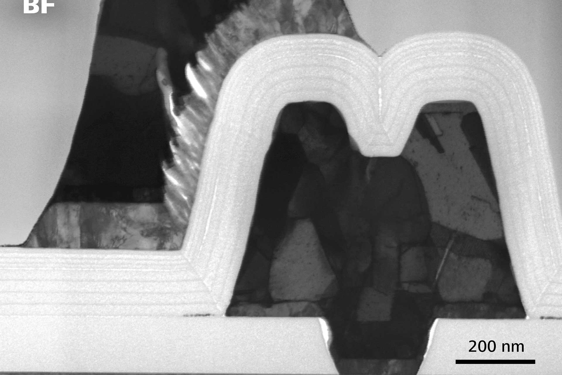
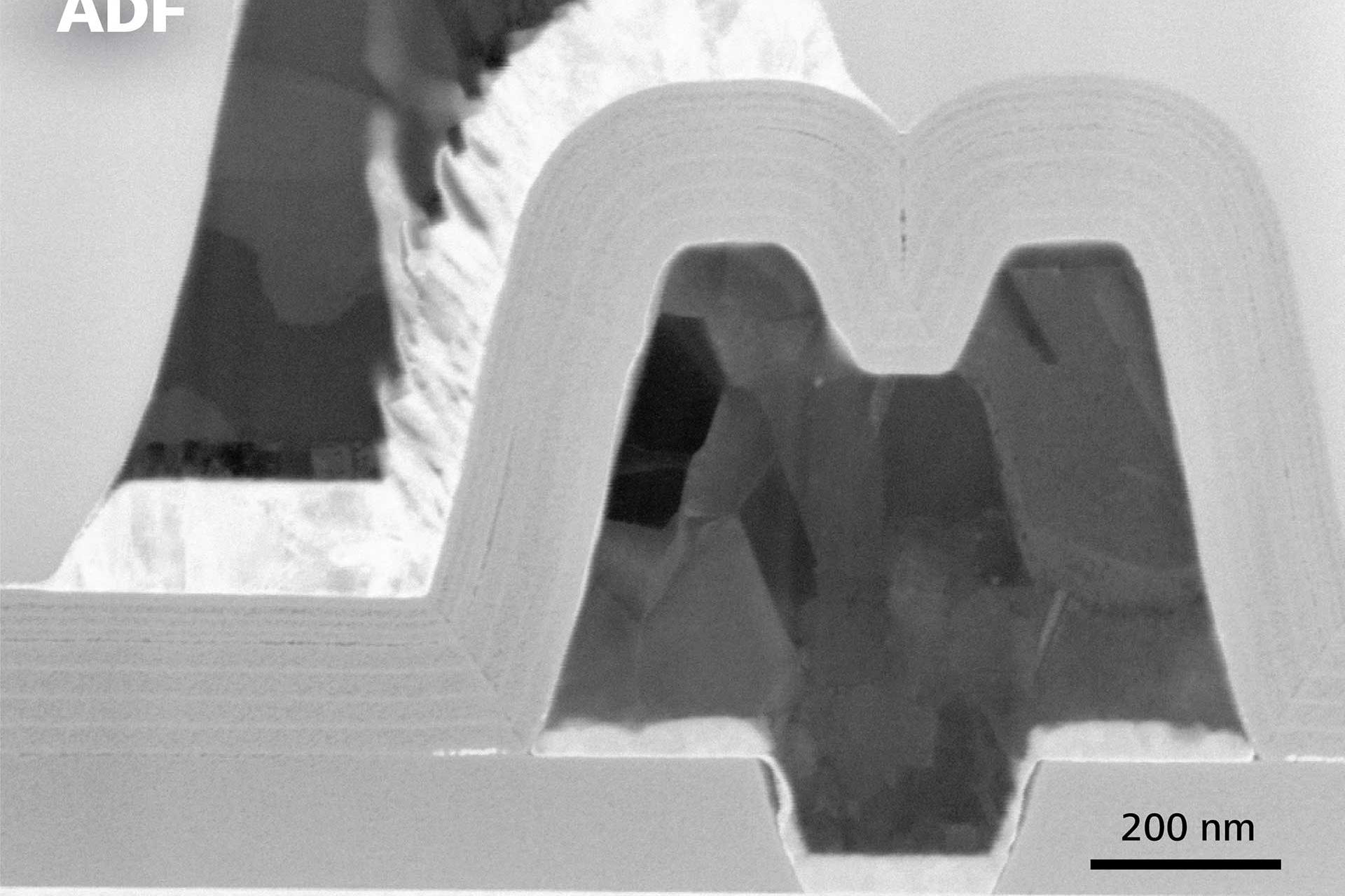
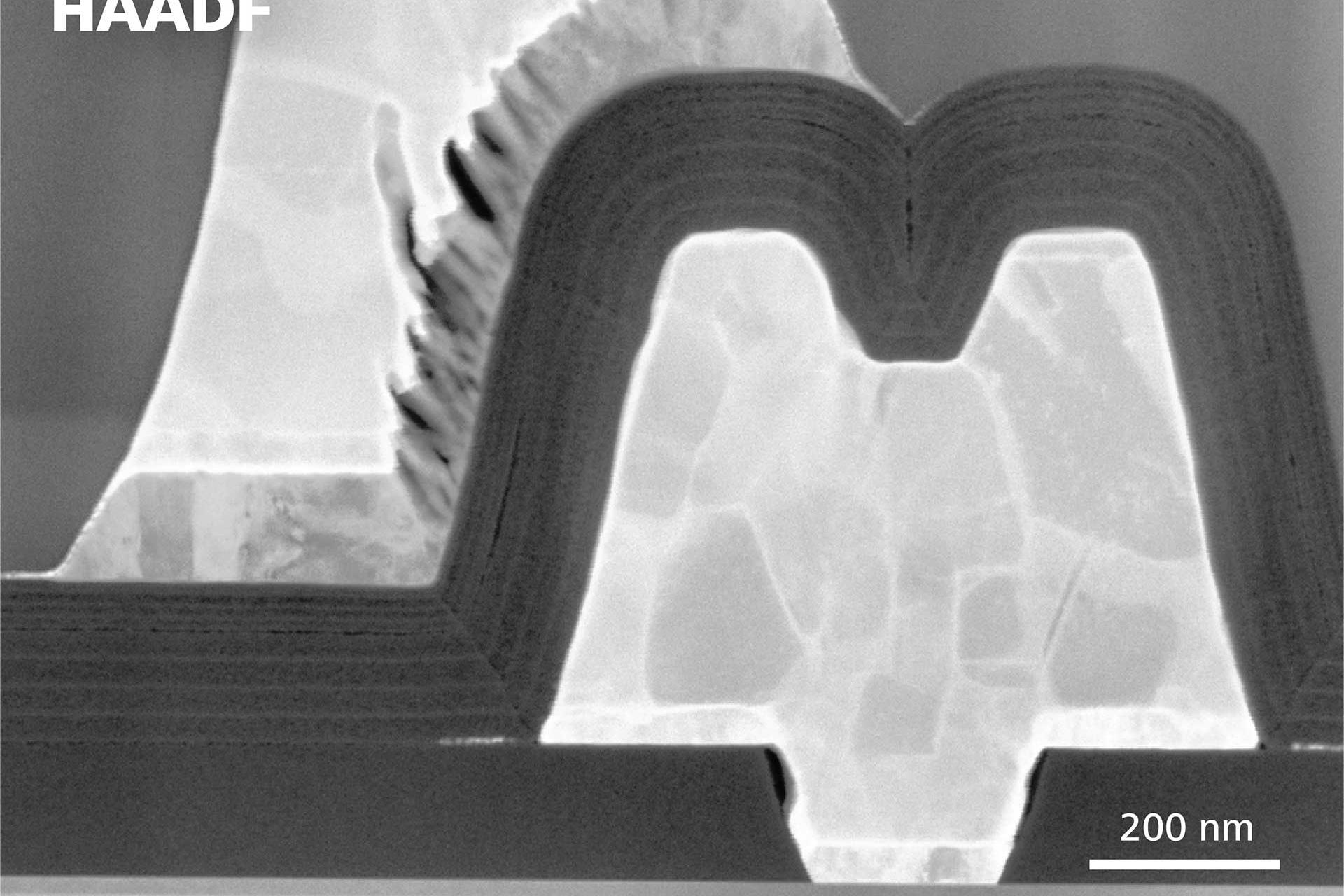
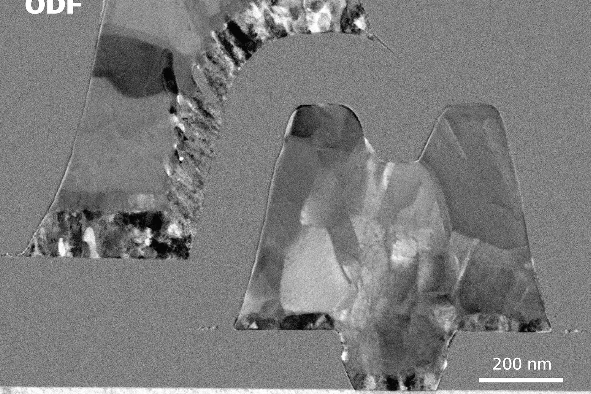
![IGBTの断面とEDX元素分析 IGBTの断面とEDX元素分析]({"xsmall":"https://www.zeiss.com/content/dam/rms/reference-master/applications/electronics-and-semiconductor/microscopy-solutions-for-semiconductor-and-electronics/insulated-gate-bipolar-transistor-cross-section-and-edx-map-fib-sem.jpg/_jcr_content/renditions/original.image_file.100.100.0,0,1920,1920.file/insulated-gate-bipolar-transistor-cross-section-and-edx-map-fib-sem.jpg","small":"https://www.zeiss.com/content/dam/rms/reference-master/applications/electronics-and-semiconductor/microscopy-solutions-for-semiconductor-and-electronics/insulated-gate-bipolar-transistor-cross-section-and-edx-map-fib-sem.jpg/_jcr_content/renditions/original.image_file.360.360.0,0,1920,1920.file/insulated-gate-bipolar-transistor-cross-section-and-edx-map-fib-sem.jpg","medium":"https://www.zeiss.com/content/dam/rms/reference-master/applications/electronics-and-semiconductor/microscopy-solutions-for-semiconductor-and-electronics/insulated-gate-bipolar-transistor-cross-section-and-edx-map-fib-sem.jpg/_jcr_content/renditions/original.image_file.768.768.0,0,1920,1920.file/insulated-gate-bipolar-transistor-cross-section-and-edx-map-fib-sem.jpg","large":"https://www.zeiss.com/content/dam/rms/reference-master/applications/electronics-and-semiconductor/microscopy-solutions-for-semiconductor-and-electronics/insulated-gate-bipolar-transistor-cross-section-and-edx-map-fib-sem.jpg/_jcr_content/renditions/original.image_file.1024.1024.0,0,1920,1920.file/insulated-gate-bipolar-transistor-cross-section-and-edx-map-fib-sem.jpg","xlarge":"https://www.zeiss.com/content/dam/rms/reference-master/applications/electronics-and-semiconductor/microscopy-solutions-for-semiconductor-and-electronics/insulated-gate-bipolar-transistor-cross-section-and-edx-map-fib-sem.jpg/_jcr_content/renditions/original.image_file.1280.1280.0,0,1920,1920.file/insulated-gate-bipolar-transistor-cross-section-and-edx-map-fib-sem.jpg","xxlarge":"https://www.zeiss.com/content/dam/rms/reference-master/applications/electronics-and-semiconductor/microscopy-solutions-for-semiconductor-and-electronics/insulated-gate-bipolar-transistor-cross-section-and-edx-map-fib-sem.jpg/_jcr_content/renditions/original.image_file.1440.1440.0,0,1920,1920.file/insulated-gate-bipolar-transistor-cross-section-and-edx-map-fib-sem.jpg","max":"https://www.zeiss.com/content/dam/rms/reference-master/applications/electronics-and-semiconductor/microscopy-solutions-for-semiconductor-and-electronics/insulated-gate-bipolar-transistor-cross-section-and-edx-map-fib-sem.jpg/_jcr_content/renditions/original.image_file.1920.1920.0,0,1920,1920.file/insulated-gate-bipolar-transistor-cross-section-and-edx-map-fib-sem.jpg"})
IGBTデバイスの断面とEDX
![IGBTの断面とEDX元素分析 IGBTの断面とEDX元素分析]({"xsmall":"https://www.zeiss.com/content/dam/rms/reference-master/applications/electronics-and-semiconductor/microscopy-solutions-for-semiconductor-and-electronics/insulated-gate-bipolar-transistor-cross-section-and-edx-map-fib-sem.jpg/_jcr_content/renditions/original.image_file.100.100.file/insulated-gate-bipolar-transistor-cross-section-and-edx-map-fib-sem.jpg","small":"https://www.zeiss.com/content/dam/rms/reference-master/applications/electronics-and-semiconductor/microscopy-solutions-for-semiconductor-and-electronics/insulated-gate-bipolar-transistor-cross-section-and-edx-map-fib-sem.jpg/_jcr_content/renditions/original.image_file.360.360.file/insulated-gate-bipolar-transistor-cross-section-and-edx-map-fib-sem.jpg","medium":"https://www.zeiss.com/content/dam/rms/reference-master/applications/electronics-and-semiconductor/microscopy-solutions-for-semiconductor-and-electronics/insulated-gate-bipolar-transistor-cross-section-and-edx-map-fib-sem.jpg/_jcr_content/renditions/original.image_file.768.768.file/insulated-gate-bipolar-transistor-cross-section-and-edx-map-fib-sem.jpg","large":"https://www.zeiss.com/content/dam/rms/reference-master/applications/electronics-and-semiconductor/microscopy-solutions-for-semiconductor-and-electronics/insulated-gate-bipolar-transistor-cross-section-and-edx-map-fib-sem.jpg/_jcr_content/renditions/original.image_file.1024.1023.file/insulated-gate-bipolar-transistor-cross-section-and-edx-map-fib-sem.jpg","xlarge":"https://www.zeiss.com/content/dam/rms/reference-master/applications/electronics-and-semiconductor/microscopy-solutions-for-semiconductor-and-electronics/insulated-gate-bipolar-transistor-cross-section-and-edx-map-fib-sem.jpg/_jcr_content/renditions/original.image_file.1280.1279.file/insulated-gate-bipolar-transistor-cross-section-and-edx-map-fib-sem.jpg","xxlarge":"https://www.zeiss.com/content/dam/rms/reference-master/applications/electronics-and-semiconductor/microscopy-solutions-for-semiconductor-and-electronics/insulated-gate-bipolar-transistor-cross-section-and-edx-map-fib-sem.jpg/_jcr_content/renditions/original.image_file.1440.1439.file/insulated-gate-bipolar-transistor-cross-section-and-edx-map-fib-sem.jpg","max":"https://www.zeiss.com/content/dam/rms/reference-master/applications/electronics-and-semiconductor/microscopy-solutions-for-semiconductor-and-electronics/insulated-gate-bipolar-transistor-cross-section-and-edx-map-fib-sem.jpg/_jcr_content/renditions/original./insulated-gate-bipolar-transistor-cross-section-and-edx-map-fib-sem.jpg"})
IGBTデバイスの断面とEDX
絶縁ゲートバイポーラトランジスタ(IGBT)のゲートの端の観察。ZEISS Crossbeam 550 FIB-SEM上で、断面解析とEDX元素分析を行いました。EDX元素分析を組み合わせたCrossbeam 30 kVでの明視野STEM-in-SEM画像で、層板表面に結晶質ケイ素析出物を認めました。
![SiC MOSFETのドーパントプロファイル SiC MOSFETのドーパントプロファイル]({"xsmall":"https://www.zeiss.com/content/dam/rms/reference-master/applications/electronics-and-semiconductor/microscopy-solutions-for-semiconductor-and-electronics/silicon-carbide-mosfet-dopant-profiling-fib-sem.jpg/_jcr_content/renditions/original.image_file.100.75.0,0,1917,1439.file/silicon-carbide-mosfet-dopant-profiling-fib-sem.jpg","small":"https://www.zeiss.com/content/dam/rms/reference-master/applications/electronics-and-semiconductor/microscopy-solutions-for-semiconductor-and-electronics/silicon-carbide-mosfet-dopant-profiling-fib-sem.jpg/_jcr_content/renditions/original.image_file.360.270.0,0,1917,1439.file/silicon-carbide-mosfet-dopant-profiling-fib-sem.jpg","medium":"https://www.zeiss.com/content/dam/rms/reference-master/applications/electronics-and-semiconductor/microscopy-solutions-for-semiconductor-and-electronics/silicon-carbide-mosfet-dopant-profiling-fib-sem.jpg/_jcr_content/renditions/original.image_file.768.576.0,0,1917,1439.file/silicon-carbide-mosfet-dopant-profiling-fib-sem.jpg","large":"https://www.zeiss.com/content/dam/rms/reference-master/applications/electronics-and-semiconductor/microscopy-solutions-for-semiconductor-and-electronics/silicon-carbide-mosfet-dopant-profiling-fib-sem.jpg/_jcr_content/renditions/original.image_file.1024.768.0,0,1917,1439.file/silicon-carbide-mosfet-dopant-profiling-fib-sem.jpg","xlarge":"https://www.zeiss.com/content/dam/rms/reference-master/applications/electronics-and-semiconductor/microscopy-solutions-for-semiconductor-and-electronics/silicon-carbide-mosfet-dopant-profiling-fib-sem.jpg/_jcr_content/renditions/original.image_file.1280.960.0,0,1917,1439.file/silicon-carbide-mosfet-dopant-profiling-fib-sem.jpg","xxlarge":"https://www.zeiss.com/content/dam/rms/reference-master/applications/electronics-and-semiconductor/microscopy-solutions-for-semiconductor-and-electronics/silicon-carbide-mosfet-dopant-profiling-fib-sem.jpg/_jcr_content/renditions/original.image_file.1440.1080.0,0,1917,1439.file/silicon-carbide-mosfet-dopant-profiling-fib-sem.jpg","max":"https://www.zeiss.com/content/dam/rms/reference-master/applications/electronics-and-semiconductor/microscopy-solutions-for-semiconductor-and-electronics/silicon-carbide-mosfet-dopant-profiling-fib-sem.jpg/_jcr_content/renditions/original.image_file.1917.1438.0,0,1917,1439.file/silicon-carbide-mosfet-dopant-profiling-fib-sem.jpg"})
SiC MOSFETのドーパントプロファイルのイメージング
![SiC MOSFETのドーパントプロファイル SiC MOSFETのドーパントプロファイル]({"xsmall":"https://www.zeiss.com/content/dam/rms/reference-master/applications/electronics-and-semiconductor/microscopy-solutions-for-semiconductor-and-electronics/silicon-carbide-mosfet-dopant-profiling-fib-sem.jpg/_jcr_content/renditions/original.image_file.100.75.file/silicon-carbide-mosfet-dopant-profiling-fib-sem.jpg","small":"https://www.zeiss.com/content/dam/rms/reference-master/applications/electronics-and-semiconductor/microscopy-solutions-for-semiconductor-and-electronics/silicon-carbide-mosfet-dopant-profiling-fib-sem.jpg/_jcr_content/renditions/original.image_file.360.270.file/silicon-carbide-mosfet-dopant-profiling-fib-sem.jpg","medium":"https://www.zeiss.com/content/dam/rms/reference-master/applications/electronics-and-semiconductor/microscopy-solutions-for-semiconductor-and-electronics/silicon-carbide-mosfet-dopant-profiling-fib-sem.jpg/_jcr_content/renditions/original.image_file.768.576.file/silicon-carbide-mosfet-dopant-profiling-fib-sem.jpg","large":"https://www.zeiss.com/content/dam/rms/reference-master/applications/electronics-and-semiconductor/microscopy-solutions-for-semiconductor-and-electronics/silicon-carbide-mosfet-dopant-profiling-fib-sem.jpg/_jcr_content/renditions/original.image_file.1024.768.file/silicon-carbide-mosfet-dopant-profiling-fib-sem.jpg","xlarge":"https://www.zeiss.com/content/dam/rms/reference-master/applications/electronics-and-semiconductor/microscopy-solutions-for-semiconductor-and-electronics/silicon-carbide-mosfet-dopant-profiling-fib-sem.jpg/_jcr_content/renditions/original.image_file.1280.960.file/silicon-carbide-mosfet-dopant-profiling-fib-sem.jpg","xxlarge":"https://www.zeiss.com/content/dam/rms/reference-master/applications/electronics-and-semiconductor/microscopy-solutions-for-semiconductor-and-electronics/silicon-carbide-mosfet-dopant-profiling-fib-sem.jpg/_jcr_content/renditions/original.image_file.1440.1080.file/silicon-carbide-mosfet-dopant-profiling-fib-sem.jpg","max":"https://www.zeiss.com/content/dam/rms/reference-master/applications/electronics-and-semiconductor/microscopy-solutions-for-semiconductor-and-electronics/silicon-carbide-mosfet-dopant-profiling-fib-sem.jpg/_jcr_content/renditions/original./silicon-carbide-mosfet-dopant-profiling-fib-sem.jpg"})
SiC MOSFETのドーパントプロファイルのイメージング
ZEISS Crossbeam FIB-SEMによって1.5 kVでイメージングした開口SiC MOSFET。画像では作用の異なる注入領域がはっきりとわかります。N型の電極はゲートに向かう濃い色のバンドとして下の方に示され、P型基板は明るい色で示されています。この方法を使うことで回路の状態や配置が明らかになります。
ナノスケールでのスマートフォン基板の3D X線イメージング
![加速度計の3D画像 - MEMS 加速度計の3D画像 - MEMS]({"xsmall":"https://www.zeiss.com/content/dam/rms/reference-master/applications/electronics-and-semiconductor/microscopy-solutions-for-semiconductor-and-electronics/smartphone-gyroscope-mems-3d-xrm.jpg/_jcr_content/renditions/original.image_file.100.100.file/smartphone-gyroscope-mems-3d-xrm.jpg","small":"https://www.zeiss.com/content/dam/rms/reference-master/applications/electronics-and-semiconductor/microscopy-solutions-for-semiconductor-and-electronics/smartphone-gyroscope-mems-3d-xrm.jpg/_jcr_content/renditions/original.image_file.360.360.file/smartphone-gyroscope-mems-3d-xrm.jpg","medium":"https://www.zeiss.com/content/dam/rms/reference-master/applications/electronics-and-semiconductor/microscopy-solutions-for-semiconductor-and-electronics/smartphone-gyroscope-mems-3d-xrm.jpg/_jcr_content/renditions/original.image_file.768.768.file/smartphone-gyroscope-mems-3d-xrm.jpg","large":"https://www.zeiss.com/content/dam/rms/reference-master/applications/electronics-and-semiconductor/microscopy-solutions-for-semiconductor-and-electronics/smartphone-gyroscope-mems-3d-xrm.jpg/_jcr_content/renditions/original.image_file.1024.1024.file/smartphone-gyroscope-mems-3d-xrm.jpg","xlarge":"https://www.zeiss.com/content/dam/rms/reference-master/applications/electronics-and-semiconductor/microscopy-solutions-for-semiconductor-and-electronics/smartphone-gyroscope-mems-3d-xrm.jpg/_jcr_content/renditions/original.image_file.1280.1280.file/smartphone-gyroscope-mems-3d-xrm.jpg","xxlarge":"https://www.zeiss.com/content/dam/rms/reference-master/applications/electronics-and-semiconductor/microscopy-solutions-for-semiconductor-and-electronics/smartphone-gyroscope-mems-3d-xrm.jpg/_jcr_content/renditions/original.image_file.1440.1440.file/smartphone-gyroscope-mems-3d-xrm.jpg","max":"https://www.zeiss.com/content/dam/rms/reference-master/applications/electronics-and-semiconductor/microscopy-solutions-for-semiconductor-and-electronics/smartphone-gyroscope-mems-3d-xrm.jpg/_jcr_content/renditions/original./smartphone-gyroscope-mems-3d-xrm.jpg"})
スマートフォンのジャイロスコープ/加速度計の3D解析
シリコンマイクロコーム構造を1 µm/ボクセルの分解能で3D X線再構築。
X線顕微鏡ZEISS Xradia Versaで取得
![加速度計のMEMSの微細フィンの平面図 加速度計のMEMSの微細フィンの平面図]({"xsmall":"https://www.zeiss.com/content/dam/rms/reference-master/applications/electronics-and-semiconductor/microscopy-solutions-for-semiconductor-and-electronics/smartphone-gyroscope-mems-fine-comb-fins-3d-xrm-plan-view.jpg/_jcr_content/renditions/original.image_file.100.100.file/smartphone-gyroscope-mems-fine-comb-fins-3d-xrm-plan-view.jpg","small":"https://www.zeiss.com/content/dam/rms/reference-master/applications/electronics-and-semiconductor/microscopy-solutions-for-semiconductor-and-electronics/smartphone-gyroscope-mems-fine-comb-fins-3d-xrm-plan-view.jpg/_jcr_content/renditions/original.image_file.360.360.file/smartphone-gyroscope-mems-fine-comb-fins-3d-xrm-plan-view.jpg","medium":"https://www.zeiss.com/content/dam/rms/reference-master/applications/electronics-and-semiconductor/microscopy-solutions-for-semiconductor-and-electronics/smartphone-gyroscope-mems-fine-comb-fins-3d-xrm-plan-view.jpg/_jcr_content/renditions/original.image_file.768.768.file/smartphone-gyroscope-mems-fine-comb-fins-3d-xrm-plan-view.jpg","large":"https://www.zeiss.com/content/dam/rms/reference-master/applications/electronics-and-semiconductor/microscopy-solutions-for-semiconductor-and-electronics/smartphone-gyroscope-mems-fine-comb-fins-3d-xrm-plan-view.jpg/_jcr_content/renditions/original.image_file.1024.1024.file/smartphone-gyroscope-mems-fine-comb-fins-3d-xrm-plan-view.jpg","xlarge":"https://www.zeiss.com/content/dam/rms/reference-master/applications/electronics-and-semiconductor/microscopy-solutions-for-semiconductor-and-electronics/smartphone-gyroscope-mems-fine-comb-fins-3d-xrm-plan-view.jpg/_jcr_content/renditions/original.image_file.1280.1280.file/smartphone-gyroscope-mems-fine-comb-fins-3d-xrm-plan-view.jpg","xxlarge":"https://www.zeiss.com/content/dam/rms/reference-master/applications/electronics-and-semiconductor/microscopy-solutions-for-semiconductor-and-electronics/smartphone-gyroscope-mems-fine-comb-fins-3d-xrm-plan-view.jpg/_jcr_content/renditions/original.image_file.1440.1440.file/smartphone-gyroscope-mems-fine-comb-fins-3d-xrm-plan-view.jpg","max":"https://www.zeiss.com/content/dam/rms/reference-master/applications/electronics-and-semiconductor/microscopy-solutions-for-semiconductor-and-electronics/smartphone-gyroscope-mems-fine-comb-fins-3d-xrm-plan-view.jpg/_jcr_content/renditions/original./smartphone-gyroscope-mems-fine-comb-fins-3d-xrm-plan-view.jpg"})
微細フィンの高解像度画像
0.3 µm/ボクセルの分解能でイメージングした同じ微細フィンの再構築平面図。
X線顕微鏡ZEISS Xradia Versaで取得
![加速度計のMEMSの微細フィンの断面図 加速度計のMEMSの微細フィンの断面図]({"xsmall":"https://www.zeiss.com/content/dam/rms/reference-master/applications/electronics-and-semiconductor/microscopy-solutions-for-semiconductor-and-electronics/smartphone-gyroscope-mems-fine-comb-fins-3d-xrm-cross-section.jpg/_jcr_content/renditions/original.image_file.100.100.file/smartphone-gyroscope-mems-fine-comb-fins-3d-xrm-cross-section.jpg","small":"https://www.zeiss.com/content/dam/rms/reference-master/applications/electronics-and-semiconductor/microscopy-solutions-for-semiconductor-and-electronics/smartphone-gyroscope-mems-fine-comb-fins-3d-xrm-cross-section.jpg/_jcr_content/renditions/original.image_file.360.360.file/smartphone-gyroscope-mems-fine-comb-fins-3d-xrm-cross-section.jpg","medium":"https://www.zeiss.com/content/dam/rms/reference-master/applications/electronics-and-semiconductor/microscopy-solutions-for-semiconductor-and-electronics/smartphone-gyroscope-mems-fine-comb-fins-3d-xrm-cross-section.jpg/_jcr_content/renditions/original.image_file.768.768.file/smartphone-gyroscope-mems-fine-comb-fins-3d-xrm-cross-section.jpg","large":"https://www.zeiss.com/content/dam/rms/reference-master/applications/electronics-and-semiconductor/microscopy-solutions-for-semiconductor-and-electronics/smartphone-gyroscope-mems-fine-comb-fins-3d-xrm-cross-section.jpg/_jcr_content/renditions/original.image_file.1024.1024.file/smartphone-gyroscope-mems-fine-comb-fins-3d-xrm-cross-section.jpg","xlarge":"https://www.zeiss.com/content/dam/rms/reference-master/applications/electronics-and-semiconductor/microscopy-solutions-for-semiconductor-and-electronics/smartphone-gyroscope-mems-fine-comb-fins-3d-xrm-cross-section.jpg/_jcr_content/renditions/original.image_file.1280.1280.file/smartphone-gyroscope-mems-fine-comb-fins-3d-xrm-cross-section.jpg","xxlarge":"https://www.zeiss.com/content/dam/rms/reference-master/applications/electronics-and-semiconductor/microscopy-solutions-for-semiconductor-and-electronics/smartphone-gyroscope-mems-fine-comb-fins-3d-xrm-cross-section.jpg/_jcr_content/renditions/original.image_file.1440.1440.file/smartphone-gyroscope-mems-fine-comb-fins-3d-xrm-cross-section.jpg","max":"https://www.zeiss.com/content/dam/rms/reference-master/applications/electronics-and-semiconductor/microscopy-solutions-for-semiconductor-and-electronics/smartphone-gyroscope-mems-fine-comb-fins-3d-xrm-cross-section.jpg/_jcr_content/renditions/original./smartphone-gyroscope-mems-fine-comb-fins-3d-xrm-cross-section.jpg"})
微細フィンの再構築スライス
0.3 µm/ボクセルの分解能でイメージングした同じ微細フィン(2.1 µm)の再構築断面図。
X線顕微鏡ZEISS Xradia Versaで取得
システム、ICパッケージ、インターコネクトの非破壊調査
![スマートフォンの3D X線イメージング スマートフォンの3D X線イメージング]({"xsmall":"https://www.zeiss.com/content/dam/rms/reference-master/applications/electronics-and-semiconductor/microscopy-solutions-for-semiconductor-and-electronics/smartphone-3d-xrm-image.jpg/_jcr_content/renditions/original.image_file.100.100.240,0,1680,1440.file/smartphone-3d-xrm-image.jpg","small":"https://www.zeiss.com/content/dam/rms/reference-master/applications/electronics-and-semiconductor/microscopy-solutions-for-semiconductor-and-electronics/smartphone-3d-xrm-image.jpg/_jcr_content/renditions/original.image_file.360.360.240,0,1680,1440.file/smartphone-3d-xrm-image.jpg","medium":"https://www.zeiss.com/content/dam/rms/reference-master/applications/electronics-and-semiconductor/microscopy-solutions-for-semiconductor-and-electronics/smartphone-3d-xrm-image.jpg/_jcr_content/renditions/original.image_file.768.768.240,0,1680,1440.file/smartphone-3d-xrm-image.jpg","large":"https://www.zeiss.com/content/dam/rms/reference-master/applications/electronics-and-semiconductor/microscopy-solutions-for-semiconductor-and-electronics/smartphone-3d-xrm-image.jpg/_jcr_content/renditions/original.image_file.1024.1024.240,0,1680,1440.file/smartphone-3d-xrm-image.jpg","xlarge":"https://www.zeiss.com/content/dam/rms/reference-master/applications/electronics-and-semiconductor/microscopy-solutions-for-semiconductor-and-electronics/smartphone-3d-xrm-image.jpg/_jcr_content/renditions/original.image_file.1280.1280.240,0,1680,1440.file/smartphone-3d-xrm-image.jpg","xxlarge":"https://www.zeiss.com/content/dam/rms/reference-master/applications/electronics-and-semiconductor/microscopy-solutions-for-semiconductor-and-electronics/smartphone-3d-xrm-image.jpg/_jcr_content/renditions/original.image_file.1440.1440.240,0,1680,1440.file/smartphone-3d-xrm-image.jpg","max":"https://www.zeiss.com/content/dam/rms/reference-master/applications/electronics-and-semiconductor/microscopy-solutions-for-semiconductor-and-electronics/smartphone-3d-xrm-image.jpg/_jcr_content/renditions/original.image_file.1440.1440.240,0,1680,1440.file/smartphone-3d-xrm-image.jpg"})
スマートフォン
![スマートフォンの3D X線イメージング スマートフォンの3D X線イメージング]({"xsmall":"https://www.zeiss.com/content/dam/rms/reference-master/applications/electronics-and-semiconductor/microscopy-solutions-for-semiconductor-and-electronics/smartphone-3d-xrm-image.jpg/_jcr_content/renditions/original.image_file.100.75.file/smartphone-3d-xrm-image.jpg","small":"https://www.zeiss.com/content/dam/rms/reference-master/applications/electronics-and-semiconductor/microscopy-solutions-for-semiconductor-and-electronics/smartphone-3d-xrm-image.jpg/_jcr_content/renditions/original.image_file.360.270.file/smartphone-3d-xrm-image.jpg","medium":"https://www.zeiss.com/content/dam/rms/reference-master/applications/electronics-and-semiconductor/microscopy-solutions-for-semiconductor-and-electronics/smartphone-3d-xrm-image.jpg/_jcr_content/renditions/original.image_file.768.576.file/smartphone-3d-xrm-image.jpg","large":"https://www.zeiss.com/content/dam/rms/reference-master/applications/electronics-and-semiconductor/microscopy-solutions-for-semiconductor-and-electronics/smartphone-3d-xrm-image.jpg/_jcr_content/renditions/original.image_file.1024.768.file/smartphone-3d-xrm-image.jpg","xlarge":"https://www.zeiss.com/content/dam/rms/reference-master/applications/electronics-and-semiconductor/microscopy-solutions-for-semiconductor-and-electronics/smartphone-3d-xrm-image.jpg/_jcr_content/renditions/original.image_file.1280.960.file/smartphone-3d-xrm-image.jpg","xxlarge":"https://www.zeiss.com/content/dam/rms/reference-master/applications/electronics-and-semiconductor/microscopy-solutions-for-semiconductor-and-electronics/smartphone-3d-xrm-image.jpg/_jcr_content/renditions/original.image_file.1440.1080.file/smartphone-3d-xrm-image.jpg","max":"https://www.zeiss.com/content/dam/rms/reference-master/applications/electronics-and-semiconductor/microscopy-solutions-for-semiconductor-and-electronics/smartphone-3d-xrm-image.jpg/_jcr_content/renditions/original./smartphone-3d-xrm-image.jpg"})
スマートフォン
スマートフォン全体を50 µm/ボクセルの分解能で3D X線イメージング。
ZEISS Xradia Context microCTで取得
![PMICパッケージの再構築平面図 PMICパッケージの再構築平面図]({"xsmall":"https://www.zeiss.com/content/dam/rms/reference-master/applications/electronics-and-semiconductor/microscopy-solutions-for-semiconductor-and-electronics/smartphone-power-management-ic-package-3d-xrm-plan-view.jpg/_jcr_content/renditions/original.image_file.100.100.482,0,1921,1439.file/smartphone-power-management-ic-package-3d-xrm-plan-view.jpg","small":"https://www.zeiss.com/content/dam/rms/reference-master/applications/electronics-and-semiconductor/microscopy-solutions-for-semiconductor-and-electronics/smartphone-power-management-ic-package-3d-xrm-plan-view.jpg/_jcr_content/renditions/original.image_file.360.360.482,0,1921,1439.file/smartphone-power-management-ic-package-3d-xrm-plan-view.jpg","medium":"https://www.zeiss.com/content/dam/rms/reference-master/applications/electronics-and-semiconductor/microscopy-solutions-for-semiconductor-and-electronics/smartphone-power-management-ic-package-3d-xrm-plan-view.jpg/_jcr_content/renditions/original.image_file.768.768.482,0,1921,1439.file/smartphone-power-management-ic-package-3d-xrm-plan-view.jpg","large":"https://www.zeiss.com/content/dam/rms/reference-master/applications/electronics-and-semiconductor/microscopy-solutions-for-semiconductor-and-electronics/smartphone-power-management-ic-package-3d-xrm-plan-view.jpg/_jcr_content/renditions/original.image_file.1024.1024.482,0,1921,1439.file/smartphone-power-management-ic-package-3d-xrm-plan-view.jpg","xlarge":"https://www.zeiss.com/content/dam/rms/reference-master/applications/electronics-and-semiconductor/microscopy-solutions-for-semiconductor-and-electronics/smartphone-power-management-ic-package-3d-xrm-plan-view.jpg/_jcr_content/renditions/original.image_file.1280.1280.482,0,1921,1439.file/smartphone-power-management-ic-package-3d-xrm-plan-view.jpg","xxlarge":"https://www.zeiss.com/content/dam/rms/reference-master/applications/electronics-and-semiconductor/microscopy-solutions-for-semiconductor-and-electronics/smartphone-power-management-ic-package-3d-xrm-plan-view.jpg/_jcr_content/renditions/original.image_file.1439.1439.482,0,1921,1439.file/smartphone-power-management-ic-package-3d-xrm-plan-view.jpg","max":"https://www.zeiss.com/content/dam/rms/reference-master/applications/electronics-and-semiconductor/microscopy-solutions-for-semiconductor-and-electronics/smartphone-power-management-ic-package-3d-xrm-plan-view.jpg/_jcr_content/renditions/original.image_file.1439.1439.482,0,1921,1439.file/smartphone-power-management-ic-package-3d-xrm-plan-view.jpg"})
電源制御ICパッケージ
![PMICパッケージの再構築平面図 PMICパッケージの再構築平面図]({"xsmall":"https://www.zeiss.com/content/dam/rms/reference-master/applications/electronics-and-semiconductor/microscopy-solutions-for-semiconductor-and-electronics/smartphone-power-management-ic-package-3d-xrm-plan-view.jpg/_jcr_content/renditions/original.image_file.100.75.file/smartphone-power-management-ic-package-3d-xrm-plan-view.jpg","small":"https://www.zeiss.com/content/dam/rms/reference-master/applications/electronics-and-semiconductor/microscopy-solutions-for-semiconductor-and-electronics/smartphone-power-management-ic-package-3d-xrm-plan-view.jpg/_jcr_content/renditions/original.image_file.360.270.file/smartphone-power-management-ic-package-3d-xrm-plan-view.jpg","medium":"https://www.zeiss.com/content/dam/rms/reference-master/applications/electronics-and-semiconductor/microscopy-solutions-for-semiconductor-and-electronics/smartphone-power-management-ic-package-3d-xrm-plan-view.jpg/_jcr_content/renditions/original.image_file.768.576.file/smartphone-power-management-ic-package-3d-xrm-plan-view.jpg","large":"https://www.zeiss.com/content/dam/rms/reference-master/applications/electronics-and-semiconductor/microscopy-solutions-for-semiconductor-and-electronics/smartphone-power-management-ic-package-3d-xrm-plan-view.jpg/_jcr_content/renditions/original.image_file.1024.768.file/smartphone-power-management-ic-package-3d-xrm-plan-view.jpg","xlarge":"https://www.zeiss.com/content/dam/rms/reference-master/applications/electronics-and-semiconductor/microscopy-solutions-for-semiconductor-and-electronics/smartphone-power-management-ic-package-3d-xrm-plan-view.jpg/_jcr_content/renditions/original.image_file.1280.960.file/smartphone-power-management-ic-package-3d-xrm-plan-view.jpg","xxlarge":"https://www.zeiss.com/content/dam/rms/reference-master/applications/electronics-and-semiconductor/microscopy-solutions-for-semiconductor-and-electronics/smartphone-power-management-ic-package-3d-xrm-plan-view.jpg/_jcr_content/renditions/original.image_file.1440.1080.file/smartphone-power-management-ic-package-3d-xrm-plan-view.jpg","max":"https://www.zeiss.com/content/dam/rms/reference-master/applications/electronics-and-semiconductor/microscopy-solutions-for-semiconductor-and-electronics/smartphone-power-management-ic-package-3d-xrm-plan-view.jpg/_jcr_content/renditions/original./smartphone-power-management-ic-package-3d-xrm-plan-view.jpg"})
電源制御ICパッケージ
11 µm/ボクセルの分解能でイメージングした電源制御ICパッケージ(PMIC)の再構築平面図。
ZEISS Xradia Context microCTで取得
![PMICパッケージのインターコネクトの断面 PMICパッケージのインターコネクトの断面]({"xsmall":"https://www.zeiss.com/content/dam/rms/reference-master/applications/electronics-and-semiconductor/microscopy-solutions-for-semiconductor-and-electronics/smartphone-power-management-ic-interconnects-3d-xrm-cross-section.jpg/_jcr_content/renditions/original.image_file.100.100.482,0,1921,1439.file/smartphone-power-management-ic-interconnects-3d-xrm-cross-section.jpg","small":"https://www.zeiss.com/content/dam/rms/reference-master/applications/electronics-and-semiconductor/microscopy-solutions-for-semiconductor-and-electronics/smartphone-power-management-ic-interconnects-3d-xrm-cross-section.jpg/_jcr_content/renditions/original.image_file.360.360.482,0,1921,1439.file/smartphone-power-management-ic-interconnects-3d-xrm-cross-section.jpg","medium":"https://www.zeiss.com/content/dam/rms/reference-master/applications/electronics-and-semiconductor/microscopy-solutions-for-semiconductor-and-electronics/smartphone-power-management-ic-interconnects-3d-xrm-cross-section.jpg/_jcr_content/renditions/original.image_file.768.768.482,0,1921,1439.file/smartphone-power-management-ic-interconnects-3d-xrm-cross-section.jpg","large":"https://www.zeiss.com/content/dam/rms/reference-master/applications/electronics-and-semiconductor/microscopy-solutions-for-semiconductor-and-electronics/smartphone-power-management-ic-interconnects-3d-xrm-cross-section.jpg/_jcr_content/renditions/original.image_file.1024.1024.482,0,1921,1439.file/smartphone-power-management-ic-interconnects-3d-xrm-cross-section.jpg","xlarge":"https://www.zeiss.com/content/dam/rms/reference-master/applications/electronics-and-semiconductor/microscopy-solutions-for-semiconductor-and-electronics/smartphone-power-management-ic-interconnects-3d-xrm-cross-section.jpg/_jcr_content/renditions/original.image_file.1280.1280.482,0,1921,1439.file/smartphone-power-management-ic-interconnects-3d-xrm-cross-section.jpg","xxlarge":"https://www.zeiss.com/content/dam/rms/reference-master/applications/electronics-and-semiconductor/microscopy-solutions-for-semiconductor-and-electronics/smartphone-power-management-ic-interconnects-3d-xrm-cross-section.jpg/_jcr_content/renditions/original.image_file.1439.1439.482,0,1921,1439.file/smartphone-power-management-ic-interconnects-3d-xrm-cross-section.jpg","max":"https://www.zeiss.com/content/dam/rms/reference-master/applications/electronics-and-semiconductor/microscopy-solutions-for-semiconductor-and-electronics/smartphone-power-management-ic-interconnects-3d-xrm-cross-section.jpg/_jcr_content/renditions/original.image_file.1439.1439.482,0,1921,1439.file/smartphone-power-management-ic-interconnects-3d-xrm-cross-section.jpg"})
PMICのインターコネクト
![PMICパッケージのインターコネクトの断面 PMICパッケージのインターコネクトの断面]({"xsmall":"https://www.zeiss.com/content/dam/rms/reference-master/applications/electronics-and-semiconductor/microscopy-solutions-for-semiconductor-and-electronics/smartphone-power-management-ic-interconnects-3d-xrm-cross-section.jpg/_jcr_content/renditions/original.image_file.100.75.file/smartphone-power-management-ic-interconnects-3d-xrm-cross-section.jpg","small":"https://www.zeiss.com/content/dam/rms/reference-master/applications/electronics-and-semiconductor/microscopy-solutions-for-semiconductor-and-electronics/smartphone-power-management-ic-interconnects-3d-xrm-cross-section.jpg/_jcr_content/renditions/original.image_file.360.270.file/smartphone-power-management-ic-interconnects-3d-xrm-cross-section.jpg","medium":"https://www.zeiss.com/content/dam/rms/reference-master/applications/electronics-and-semiconductor/microscopy-solutions-for-semiconductor-and-electronics/smartphone-power-management-ic-interconnects-3d-xrm-cross-section.jpg/_jcr_content/renditions/original.image_file.768.576.file/smartphone-power-management-ic-interconnects-3d-xrm-cross-section.jpg","large":"https://www.zeiss.com/content/dam/rms/reference-master/applications/electronics-and-semiconductor/microscopy-solutions-for-semiconductor-and-electronics/smartphone-power-management-ic-interconnects-3d-xrm-cross-section.jpg/_jcr_content/renditions/original.image_file.1024.768.file/smartphone-power-management-ic-interconnects-3d-xrm-cross-section.jpg","xlarge":"https://www.zeiss.com/content/dam/rms/reference-master/applications/electronics-and-semiconductor/microscopy-solutions-for-semiconductor-and-electronics/smartphone-power-management-ic-interconnects-3d-xrm-cross-section.jpg/_jcr_content/renditions/original.image_file.1280.960.file/smartphone-power-management-ic-interconnects-3d-xrm-cross-section.jpg","xxlarge":"https://www.zeiss.com/content/dam/rms/reference-master/applications/electronics-and-semiconductor/microscopy-solutions-for-semiconductor-and-electronics/smartphone-power-management-ic-interconnects-3d-xrm-cross-section.jpg/_jcr_content/renditions/original.image_file.1440.1080.file/smartphone-power-management-ic-interconnects-3d-xrm-cross-section.jpg","max":"https://www.zeiss.com/content/dam/rms/reference-master/applications/electronics-and-semiconductor/microscopy-solutions-for-semiconductor-and-electronics/smartphone-power-management-ic-interconnects-3d-xrm-cross-section.jpg/_jcr_content/renditions/original./smartphone-power-management-ic-interconnects-3d-xrm-cross-section.jpg"})
PMICインターコネクトの断面
2.1 µm/ボクセルの分解能でイメージングしたPMICのソルダーバンプとビアの再構築断面図。
X線顕微鏡ZEISS Xradia Versaの独自機能Resolution at a Distanceを使用して取得。
EBACによるアナログチップのイメージング
GeminiSEMで、ナノプロービング技術を使って20 kVで観察した電子アナログチップ。電子ビーム吸収電流(EBAC)イメージングからは、内部の配線とpn接合の相互接続に関する情報が得られます。