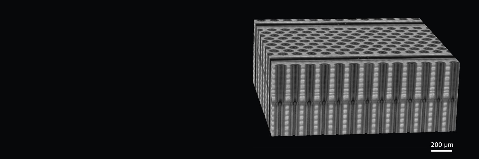
Use Case

Logic and Memory Research

Explore the future of semiconductors with our latest article on logic and memory advancements.

Dive into the details of state-of-the-art microscopy techniques driving the next generation of electronic devices.

Electronics Research

Unveiling Logic and Memory Potential

  • Logic and Memory
  • Logic and Memory
  • Logic and Memory
  • Logic and Memory
  • Logic and Memory
  • Logic and Memory

Leading the Charge in Microscopic Innovations

In the fast-evolving semiconductor industry, the demand for increased computing power and smaller form factors is met with innovations in logic and memory devices. This article delves into the challenges and solutions associated with analyzing these critical components. With shrinking transistor sizes, traditional characterization methods no longer suffice. We discuss the application of advanced microscopy techniques, including FE-SEM and FIB-SEM, to achieve high throughput and success rates essential for device development and failure analysis. The use of low-energy beams and large working distances helps protect delicate semiconductor materials during analysis, ensuring accurate results without compromising the integrity of the sample. Furthermore, connected tools and automated solutions enhance efficiency across global supply chains, contributing to faster development cycles and improved yield. Through expert insights and case studies, the article showcases how cutting-edge microscopy solutions are pivotal in navigating the complexities of novel materials and intricate device architectures, ultimately accelerating the pace of innovation in the semiconductor sector.


Complete your lab

with our new solution bundles

You can enhance your Logic and Memory Research with the following solutions

High End Microscopy

with the ZEISS Crossbeam

Crossbeam 550 system

ZEISS Crossbeam​

FIB-SEM for High Throughput 3D Analysis and Sample Preparation​

ZEISS microscopy solutions are pivotal in advancing the semiconductor industry, especially for logic and memory applications. With the demand for higher computing performance in ever-smaller devices, ZEISS provides critical tools like the GeminiSEM and Crossbeam series, designed for high-resolution, non-destructive imaging and analysis. These systems facilitate complex structural and electrical characterizations at sub-nanometer scales, driving innovations in materials and process development. By leveraging ZEISS's advanced microscopy technologies, industry professionals can achieve faster failure analysis, enhanced productivity, and superior device performance.
 

Electronics Research Articles