
Advanced Microscopy for Electronic Materials & Semiconductor Packages
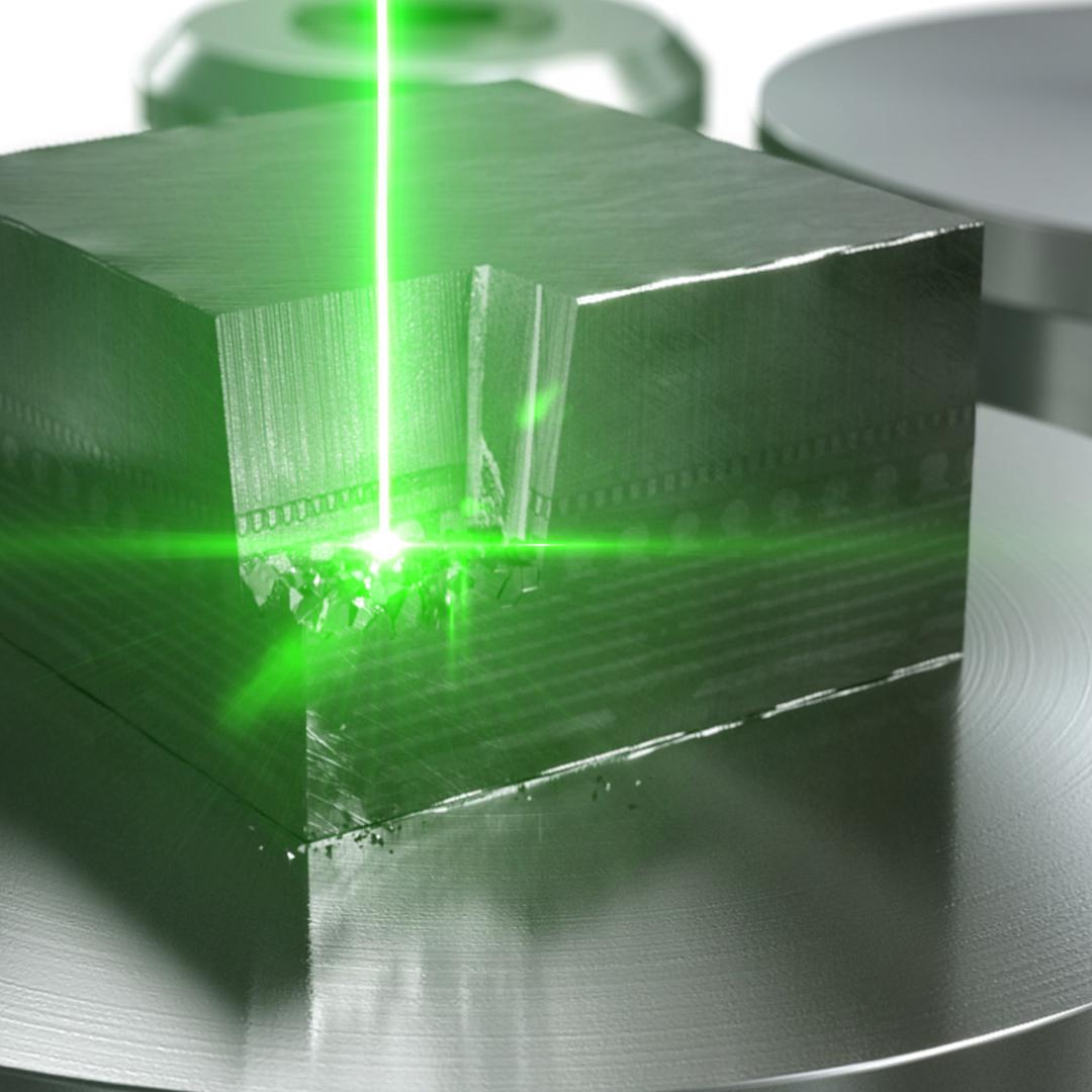
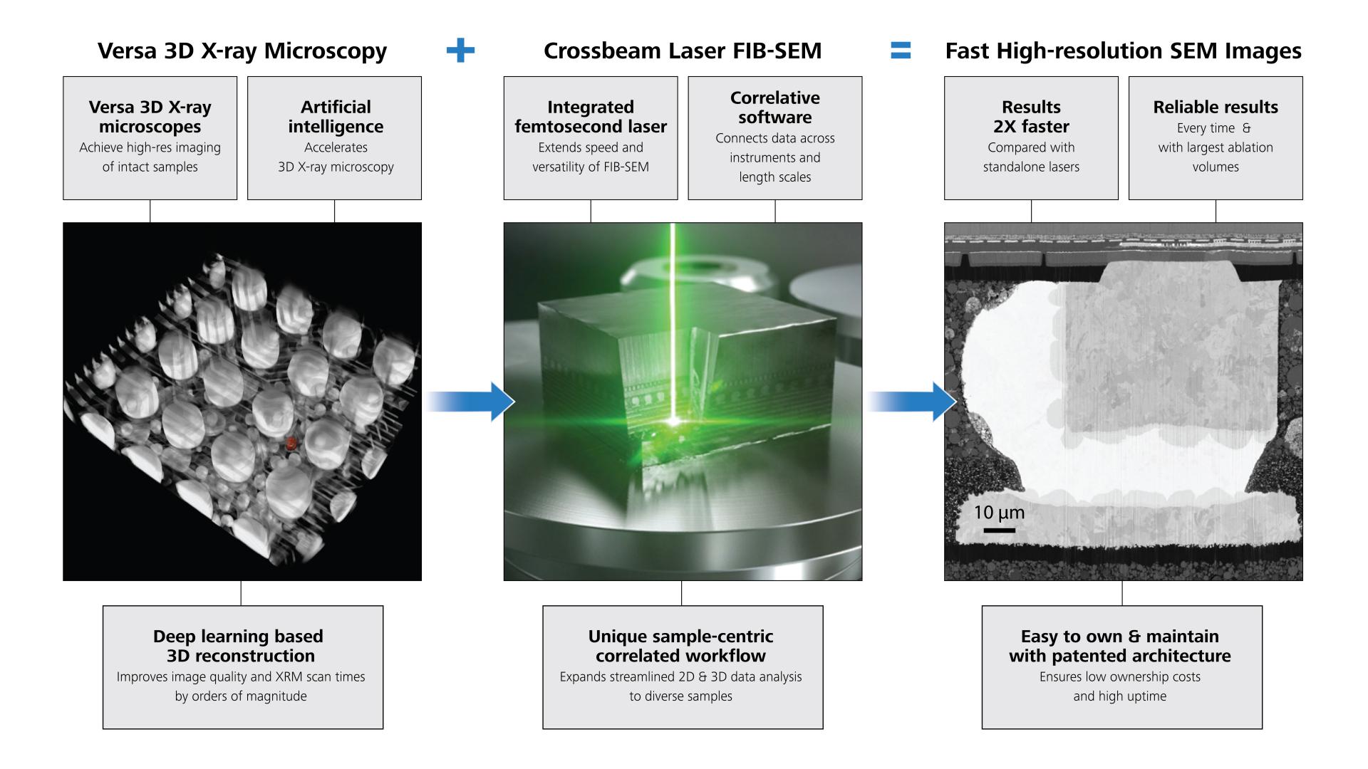
Parallel advances in FIB-SEM and 3D X-ray microscopy have radically changed sample preparation, characterization and failure analysis of semiconductor devices and packages.
Learn more by interacting with the flashing dots
Transform Your Sample Prep and Site-specific Analysis with Efficient Workflows

New Technology Insights for Materials Characterization & Failure Analysis
Two webinars deliver rich insights into the latest microscopy advances and how they work together to enable materials characterization and failure analysis for the next generation of electronic packages and devices.

Explore Related Applications


How can we help you?
Contact us to speak directly with a ZEISS representative about the specific needs of your facility.