![模拟微芯片和封装 模拟微芯片和封装]({"xsmall":"https://www.zeiss.com/content/dam/rms/reference-master/applications/electronics-and-semiconductor/microscopy-solutions-for-semiconductor-and-electronics/analog-rf-power-mems-sensors-microscopy-solutions.jpg/_jcr_content/renditions/original.image_file.100.100.240,0,1680,1440.file/analog-rf-power-mems-sensors-microscopy-solutions.jpg","small":"https://www.zeiss.com/content/dam/rms/reference-master/applications/electronics-and-semiconductor/microscopy-solutions-for-semiconductor-and-electronics/analog-rf-power-mems-sensors-microscopy-solutions.jpg/_jcr_content/renditions/original.image_file.360.360.240,0,1680,1440.file/analog-rf-power-mems-sensors-microscopy-solutions.jpg","medium":"https://www.zeiss.com/content/dam/rms/reference-master/applications/electronics-and-semiconductor/microscopy-solutions-for-semiconductor-and-electronics/analog-rf-power-mems-sensors-microscopy-solutions.jpg/_jcr_content/renditions/original.image_file.768.768.240,0,1680,1440.file/analog-rf-power-mems-sensors-microscopy-solutions.jpg","large":"https://www.zeiss.com/content/dam/rms/reference-master/applications/electronics-and-semiconductor/microscopy-solutions-for-semiconductor-and-electronics/analog-rf-power-mems-sensors-microscopy-solutions.jpg/_jcr_content/renditions/original.image_file.1024.1024.240,0,1680,1440.file/analog-rf-power-mems-sensors-microscopy-solutions.jpg","xlarge":"https://www.zeiss.com/content/dam/rms/reference-master/applications/electronics-and-semiconductor/microscopy-solutions-for-semiconductor-and-electronics/analog-rf-power-mems-sensors-microscopy-solutions.jpg/_jcr_content/renditions/original.image_file.1280.1280.240,0,1680,1440.file/analog-rf-power-mems-sensors-microscopy-solutions.jpg","xxlarge":"https://www.zeiss.com/content/dam/rms/reference-master/applications/electronics-and-semiconductor/microscopy-solutions-for-semiconductor-and-electronics/analog-rf-power-mems-sensors-microscopy-solutions.jpg/_jcr_content/renditions/original.image_file.1440.1440.240,0,1680,1440.file/analog-rf-power-mems-sensors-microscopy-solutions.jpg","max":"https://www.zeiss.com/content/dam/rms/reference-master/applications/electronics-and-semiconductor/microscopy-solutions-for-semiconductor-and-electronics/analog-rf-power-mems-sensors-microscopy-solutions.jpg/_jcr_content/renditions/original.image_file.1440.1440.240,0,1680,1440.file/analog-rf-power-mems-sensors-microscopy-solutions.jpg"})
对复杂新材料和结构进行高级分析
通过准确的失效分析加快上市
移动通信、物联网(IoT)、云计算和汽车行业电气化致使对高性能“超摩尔”半导体器件的需求与日俱增,其需要集成新材料和工艺,或新型硅架构和封装技术,例如微机电系统(MEMS)。砷化镓(GaAs)、碳化硅(SiC)和氮化镓(GaN)等直接带隙和宽带隙材料对设备制造商和器件装配商等提出了新的挑战。其中许多器件还集成了传统IC,给装配和封装带来了困难。
为了缩短这些复杂器件的开发周期并加快上市,制造商需要先进的分析工具来支持复杂的新材料集成和失效根本原因分析。
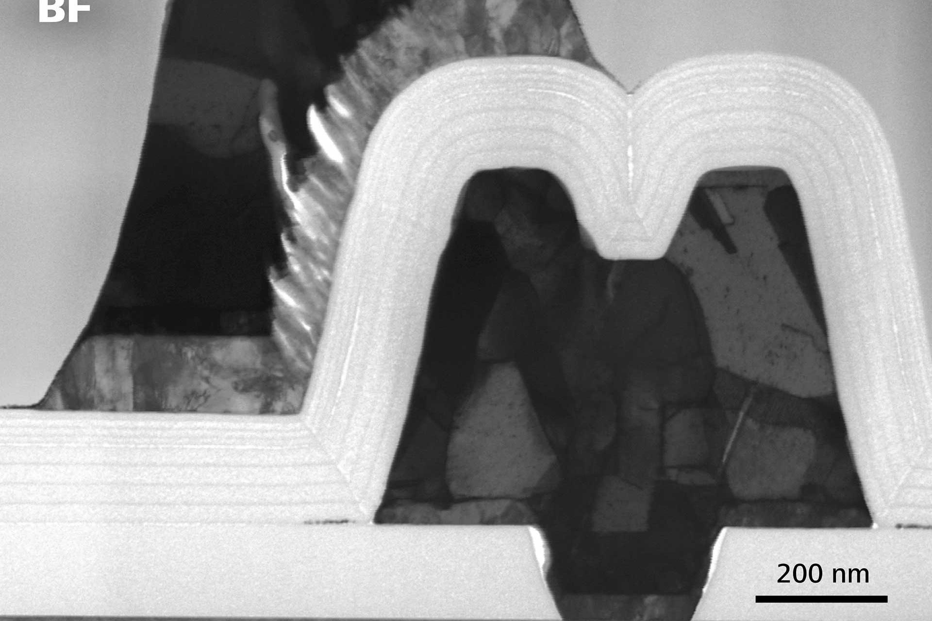
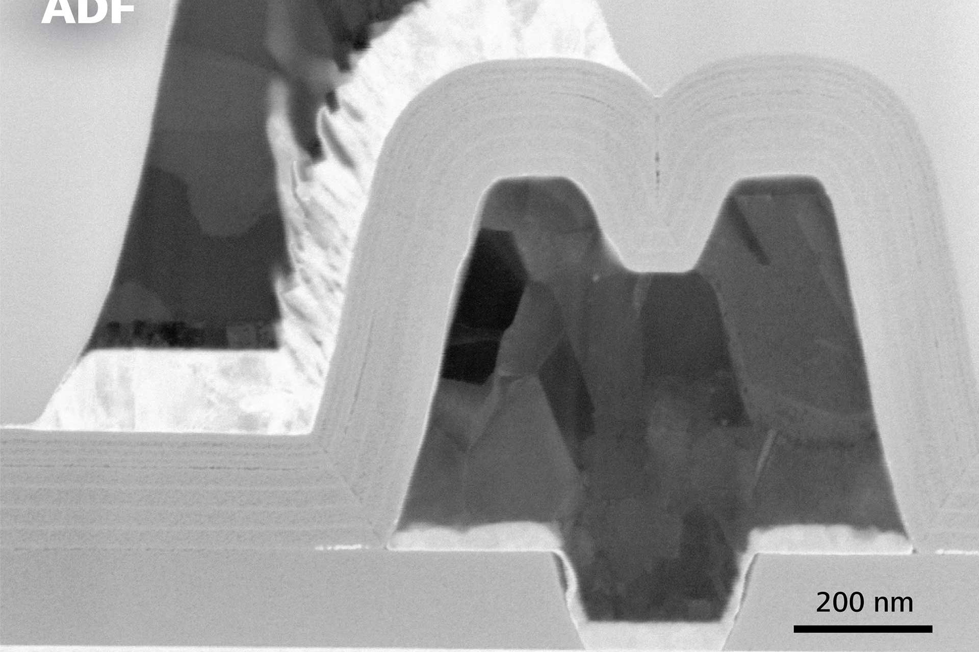
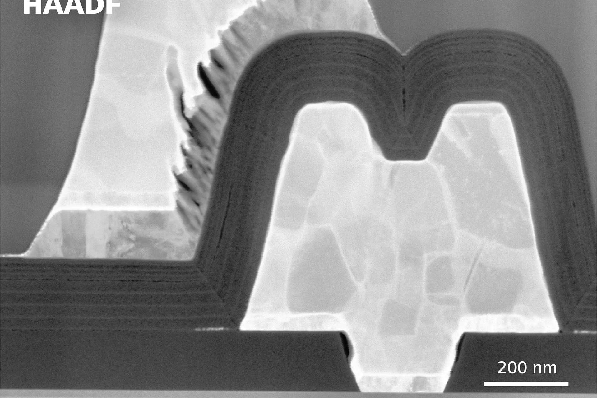
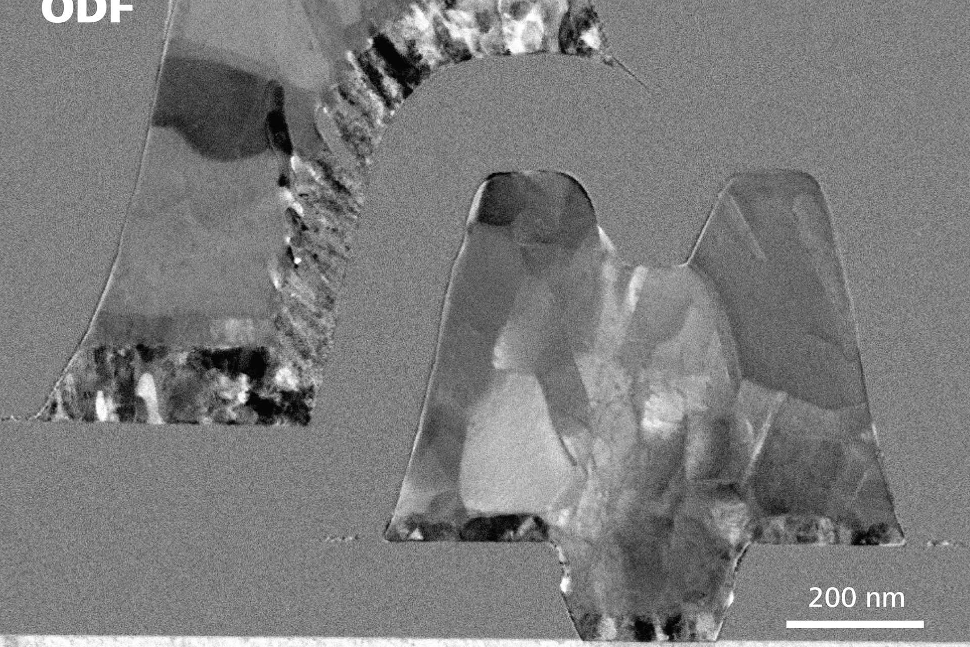
![IGBT截面和EDS面分布图 IGBT截面和EDS面分布图]({"xsmall":"https://www.zeiss.com/content/dam/rms/reference-master/applications/electronics-and-semiconductor/microscopy-solutions-for-semiconductor-and-electronics/insulated-gate-bipolar-transistor-cross-section-and-edx-map-fib-sem.jpg/_jcr_content/renditions/original.image_file.100.100.0,0,1920,1920.file/insulated-gate-bipolar-transistor-cross-section-and-edx-map-fib-sem.jpg","small":"https://www.zeiss.com/content/dam/rms/reference-master/applications/electronics-and-semiconductor/microscopy-solutions-for-semiconductor-and-electronics/insulated-gate-bipolar-transistor-cross-section-and-edx-map-fib-sem.jpg/_jcr_content/renditions/original.image_file.360.360.0,0,1920,1920.file/insulated-gate-bipolar-transistor-cross-section-and-edx-map-fib-sem.jpg","medium":"https://www.zeiss.com/content/dam/rms/reference-master/applications/electronics-and-semiconductor/microscopy-solutions-for-semiconductor-and-electronics/insulated-gate-bipolar-transistor-cross-section-and-edx-map-fib-sem.jpg/_jcr_content/renditions/original.image_file.768.768.0,0,1920,1920.file/insulated-gate-bipolar-transistor-cross-section-and-edx-map-fib-sem.jpg","large":"https://www.zeiss.com/content/dam/rms/reference-master/applications/electronics-and-semiconductor/microscopy-solutions-for-semiconductor-and-electronics/insulated-gate-bipolar-transistor-cross-section-and-edx-map-fib-sem.jpg/_jcr_content/renditions/original.image_file.1024.1024.0,0,1920,1920.file/insulated-gate-bipolar-transistor-cross-section-and-edx-map-fib-sem.jpg","xlarge":"https://www.zeiss.com/content/dam/rms/reference-master/applications/electronics-and-semiconductor/microscopy-solutions-for-semiconductor-and-electronics/insulated-gate-bipolar-transistor-cross-section-and-edx-map-fib-sem.jpg/_jcr_content/renditions/original.image_file.1280.1280.0,0,1920,1920.file/insulated-gate-bipolar-transistor-cross-section-and-edx-map-fib-sem.jpg","xxlarge":"https://www.zeiss.com/content/dam/rms/reference-master/applications/electronics-and-semiconductor/microscopy-solutions-for-semiconductor-and-electronics/insulated-gate-bipolar-transistor-cross-section-and-edx-map-fib-sem.jpg/_jcr_content/renditions/original.image_file.1440.1440.0,0,1920,1920.file/insulated-gate-bipolar-transistor-cross-section-and-edx-map-fib-sem.jpg","max":"https://www.zeiss.com/content/dam/rms/reference-master/applications/electronics-and-semiconductor/microscopy-solutions-for-semiconductor-and-electronics/insulated-gate-bipolar-transistor-cross-section-and-edx-map-fib-sem.jpg/_jcr_content/renditions/original.image_file.1920.1920.0,0,1920,1920.file/insulated-gate-bipolar-transistor-cross-section-and-edx-map-fib-sem.jpg"})
IGBT器件的截面和EDS
![IGBT截面和EDS面分布图 IGBT截面和EDS面分布图]({"xsmall":"https://www.zeiss.com/content/dam/rms/reference-master/applications/electronics-and-semiconductor/microscopy-solutions-for-semiconductor-and-electronics/insulated-gate-bipolar-transistor-cross-section-and-edx-map-fib-sem.jpg/_jcr_content/renditions/original.image_file.100.100.file/insulated-gate-bipolar-transistor-cross-section-and-edx-map-fib-sem.jpg","small":"https://www.zeiss.com/content/dam/rms/reference-master/applications/electronics-and-semiconductor/microscopy-solutions-for-semiconductor-and-electronics/insulated-gate-bipolar-transistor-cross-section-and-edx-map-fib-sem.jpg/_jcr_content/renditions/original.image_file.360.360.file/insulated-gate-bipolar-transistor-cross-section-and-edx-map-fib-sem.jpg","medium":"https://www.zeiss.com/content/dam/rms/reference-master/applications/electronics-and-semiconductor/microscopy-solutions-for-semiconductor-and-electronics/insulated-gate-bipolar-transistor-cross-section-and-edx-map-fib-sem.jpg/_jcr_content/renditions/original.image_file.768.768.file/insulated-gate-bipolar-transistor-cross-section-and-edx-map-fib-sem.jpg","large":"https://www.zeiss.com/content/dam/rms/reference-master/applications/electronics-and-semiconductor/microscopy-solutions-for-semiconductor-and-electronics/insulated-gate-bipolar-transistor-cross-section-and-edx-map-fib-sem.jpg/_jcr_content/renditions/original.image_file.1024.1023.file/insulated-gate-bipolar-transistor-cross-section-and-edx-map-fib-sem.jpg","xlarge":"https://www.zeiss.com/content/dam/rms/reference-master/applications/electronics-and-semiconductor/microscopy-solutions-for-semiconductor-and-electronics/insulated-gate-bipolar-transistor-cross-section-and-edx-map-fib-sem.jpg/_jcr_content/renditions/original.image_file.1280.1279.file/insulated-gate-bipolar-transistor-cross-section-and-edx-map-fib-sem.jpg","xxlarge":"https://www.zeiss.com/content/dam/rms/reference-master/applications/electronics-and-semiconductor/microscopy-solutions-for-semiconductor-and-electronics/insulated-gate-bipolar-transistor-cross-section-and-edx-map-fib-sem.jpg/_jcr_content/renditions/original.image_file.1440.1439.file/insulated-gate-bipolar-transistor-cross-section-and-edx-map-fib-sem.jpg","max":"https://www.zeiss.com/content/dam/rms/reference-master/applications/electronics-and-semiconductor/microscopy-solutions-for-semiconductor-and-electronics/insulated-gate-bipolar-transistor-cross-section-and-edx-map-fib-sem.jpg/_jcr_content/renditions/original./insulated-gate-bipolar-transistor-cross-section-and-edx-map-fib-sem.jpg"})
IGBT器件的截面和EDS
绝缘栅双极晶体管(IGBT)器件栅极边缘检查。截面和EDS元素分析全部在蔡司Crossbeam 550 FIB-SEM上完成。薄片的明场30 kV STEM-in-SEM图像与Crossbeam中的EDS元素面分布成像相结合,揭示了晶体硅沉淀物。
![碳化硅MOSFET掺杂分布 碳化硅MOSFET掺杂分布]({"xsmall":"https://www.zeiss.com/content/dam/rms/reference-master/applications/electronics-and-semiconductor/microscopy-solutions-for-semiconductor-and-electronics/silicon-carbide-mosfet-dopant-profiling-fib-sem.jpg/_jcr_content/renditions/original.image_file.100.75.0,0,1917,1439.file/silicon-carbide-mosfet-dopant-profiling-fib-sem.jpg","small":"https://www.zeiss.com/content/dam/rms/reference-master/applications/electronics-and-semiconductor/microscopy-solutions-for-semiconductor-and-electronics/silicon-carbide-mosfet-dopant-profiling-fib-sem.jpg/_jcr_content/renditions/original.image_file.360.270.0,0,1917,1439.file/silicon-carbide-mosfet-dopant-profiling-fib-sem.jpg","medium":"https://www.zeiss.com/content/dam/rms/reference-master/applications/electronics-and-semiconductor/microscopy-solutions-for-semiconductor-and-electronics/silicon-carbide-mosfet-dopant-profiling-fib-sem.jpg/_jcr_content/renditions/original.image_file.768.576.0,0,1917,1439.file/silicon-carbide-mosfet-dopant-profiling-fib-sem.jpg","large":"https://www.zeiss.com/content/dam/rms/reference-master/applications/electronics-and-semiconductor/microscopy-solutions-for-semiconductor-and-electronics/silicon-carbide-mosfet-dopant-profiling-fib-sem.jpg/_jcr_content/renditions/original.image_file.1024.768.0,0,1917,1439.file/silicon-carbide-mosfet-dopant-profiling-fib-sem.jpg","xlarge":"https://www.zeiss.com/content/dam/rms/reference-master/applications/electronics-and-semiconductor/microscopy-solutions-for-semiconductor-and-electronics/silicon-carbide-mosfet-dopant-profiling-fib-sem.jpg/_jcr_content/renditions/original.image_file.1280.960.0,0,1917,1439.file/silicon-carbide-mosfet-dopant-profiling-fib-sem.jpg","xxlarge":"https://www.zeiss.com/content/dam/rms/reference-master/applications/electronics-and-semiconductor/microscopy-solutions-for-semiconductor-and-electronics/silicon-carbide-mosfet-dopant-profiling-fib-sem.jpg/_jcr_content/renditions/original.image_file.1440.1080.0,0,1917,1439.file/silicon-carbide-mosfet-dopant-profiling-fib-sem.jpg","max":"https://www.zeiss.com/content/dam/rms/reference-master/applications/electronics-and-semiconductor/microscopy-solutions-for-semiconductor-and-electronics/silicon-carbide-mosfet-dopant-profiling-fib-sem.jpg/_jcr_content/renditions/original.image_file.1917.1438.0,0,1917,1439.file/silicon-carbide-mosfet-dopant-profiling-fib-sem.jpg"})
碳化硅MOSFET掺杂分布图
![碳化硅MOSFET掺杂分布 碳化硅MOSFET掺杂分布]({"xsmall":"https://www.zeiss.com/content/dam/rms/reference-master/applications/electronics-and-semiconductor/microscopy-solutions-for-semiconductor-and-electronics/silicon-carbide-mosfet-dopant-profiling-fib-sem.jpg/_jcr_content/renditions/original.image_file.100.75.file/silicon-carbide-mosfet-dopant-profiling-fib-sem.jpg","small":"https://www.zeiss.com/content/dam/rms/reference-master/applications/electronics-and-semiconductor/microscopy-solutions-for-semiconductor-and-electronics/silicon-carbide-mosfet-dopant-profiling-fib-sem.jpg/_jcr_content/renditions/original.image_file.360.270.file/silicon-carbide-mosfet-dopant-profiling-fib-sem.jpg","medium":"https://www.zeiss.com/content/dam/rms/reference-master/applications/electronics-and-semiconductor/microscopy-solutions-for-semiconductor-and-electronics/silicon-carbide-mosfet-dopant-profiling-fib-sem.jpg/_jcr_content/renditions/original.image_file.768.576.file/silicon-carbide-mosfet-dopant-profiling-fib-sem.jpg","large":"https://www.zeiss.com/content/dam/rms/reference-master/applications/electronics-and-semiconductor/microscopy-solutions-for-semiconductor-and-electronics/silicon-carbide-mosfet-dopant-profiling-fib-sem.jpg/_jcr_content/renditions/original.image_file.1024.768.file/silicon-carbide-mosfet-dopant-profiling-fib-sem.jpg","xlarge":"https://www.zeiss.com/content/dam/rms/reference-master/applications/electronics-and-semiconductor/microscopy-solutions-for-semiconductor-and-electronics/silicon-carbide-mosfet-dopant-profiling-fib-sem.jpg/_jcr_content/renditions/original.image_file.1280.960.file/silicon-carbide-mosfet-dopant-profiling-fib-sem.jpg","xxlarge":"https://www.zeiss.com/content/dam/rms/reference-master/applications/electronics-and-semiconductor/microscopy-solutions-for-semiconductor-and-electronics/silicon-carbide-mosfet-dopant-profiling-fib-sem.jpg/_jcr_content/renditions/original.image_file.1440.1080.file/silicon-carbide-mosfet-dopant-profiling-fib-sem.jpg","max":"https://www.zeiss.com/content/dam/rms/reference-master/applications/electronics-and-semiconductor/microscopy-solutions-for-semiconductor-and-electronics/silicon-carbide-mosfet-dopant-profiling-fib-sem.jpg/_jcr_content/renditions/original./silicon-carbide-mosfet-dopant-profiling-fib-sem.jpg"})
碳化硅MOSFET掺杂分布图
裂解碳化硅MOSFET器件,使用蔡司Crossbeam FIB-SEM在1.5 kV电压下成像。由于功函数的差异,该图像明显突出了不同的注入掺杂区域。N+扩散显示为下方的暗带,并延伸至栅极的任一侧。P型主体掺杂区突出显示为亮区。此技术提供有关结点健康状况和布置的反馈。
智能手机主板的纳米级三维X射线成像
![加速度计的三维图像——MEMS 加速度计的三维图像——MEMS]({"xsmall":"https://www.zeiss.com/content/dam/rms/reference-master/applications/electronics-and-semiconductor/microscopy-solutions-for-semiconductor-and-electronics/smartphone-gyroscope-mems-3d-xrm.jpg/_jcr_content/renditions/original.image_file.100.100.file/smartphone-gyroscope-mems-3d-xrm.jpg","small":"https://www.zeiss.com/content/dam/rms/reference-master/applications/electronics-and-semiconductor/microscopy-solutions-for-semiconductor-and-electronics/smartphone-gyroscope-mems-3d-xrm.jpg/_jcr_content/renditions/original.image_file.360.360.file/smartphone-gyroscope-mems-3d-xrm.jpg","medium":"https://www.zeiss.com/content/dam/rms/reference-master/applications/electronics-and-semiconductor/microscopy-solutions-for-semiconductor-and-electronics/smartphone-gyroscope-mems-3d-xrm.jpg/_jcr_content/renditions/original.image_file.768.768.file/smartphone-gyroscope-mems-3d-xrm.jpg","large":"https://www.zeiss.com/content/dam/rms/reference-master/applications/electronics-and-semiconductor/microscopy-solutions-for-semiconductor-and-electronics/smartphone-gyroscope-mems-3d-xrm.jpg/_jcr_content/renditions/original.image_file.1024.1024.file/smartphone-gyroscope-mems-3d-xrm.jpg","xlarge":"https://www.zeiss.com/content/dam/rms/reference-master/applications/electronics-and-semiconductor/microscopy-solutions-for-semiconductor-and-electronics/smartphone-gyroscope-mems-3d-xrm.jpg/_jcr_content/renditions/original.image_file.1280.1280.file/smartphone-gyroscope-mems-3d-xrm.jpg","xxlarge":"https://www.zeiss.com/content/dam/rms/reference-master/applications/electronics-and-semiconductor/microscopy-solutions-for-semiconductor-and-electronics/smartphone-gyroscope-mems-3d-xrm.jpg/_jcr_content/renditions/original.image_file.1440.1440.file/smartphone-gyroscope-mems-3d-xrm.jpg","max":"https://www.zeiss.com/content/dam/rms/reference-master/applications/electronics-and-semiconductor/microscopy-solutions-for-semiconductor-and-electronics/smartphone-gyroscope-mems-3d-xrm.jpg/_jcr_content/renditions/original./smartphone-gyroscope-mems-3d-xrm.jpg"})
智能手机陀螺仪/加速度计的三维分析
硅微梳结构的三维X射线重构,以1 µm/体素的分辨率成像。
使用蔡司Xradia Versa X射线显微镜成像
![加速度计MEMS精细梳状鳍片的平面图 加速度计MEMS精细梳状鳍片的平面图]({"xsmall":"https://www.zeiss.com/content/dam/rms/reference-master/applications/electronics-and-semiconductor/microscopy-solutions-for-semiconductor-and-electronics/smartphone-gyroscope-mems-fine-comb-fins-3d-xrm-plan-view.jpg/_jcr_content/renditions/original.image_file.100.100.file/smartphone-gyroscope-mems-fine-comb-fins-3d-xrm-plan-view.jpg","small":"https://www.zeiss.com/content/dam/rms/reference-master/applications/electronics-and-semiconductor/microscopy-solutions-for-semiconductor-and-electronics/smartphone-gyroscope-mems-fine-comb-fins-3d-xrm-plan-view.jpg/_jcr_content/renditions/original.image_file.360.360.file/smartphone-gyroscope-mems-fine-comb-fins-3d-xrm-plan-view.jpg","medium":"https://www.zeiss.com/content/dam/rms/reference-master/applications/electronics-and-semiconductor/microscopy-solutions-for-semiconductor-and-electronics/smartphone-gyroscope-mems-fine-comb-fins-3d-xrm-plan-view.jpg/_jcr_content/renditions/original.image_file.768.768.file/smartphone-gyroscope-mems-fine-comb-fins-3d-xrm-plan-view.jpg","large":"https://www.zeiss.com/content/dam/rms/reference-master/applications/electronics-and-semiconductor/microscopy-solutions-for-semiconductor-and-electronics/smartphone-gyroscope-mems-fine-comb-fins-3d-xrm-plan-view.jpg/_jcr_content/renditions/original.image_file.1024.1024.file/smartphone-gyroscope-mems-fine-comb-fins-3d-xrm-plan-view.jpg","xlarge":"https://www.zeiss.com/content/dam/rms/reference-master/applications/electronics-and-semiconductor/microscopy-solutions-for-semiconductor-and-electronics/smartphone-gyroscope-mems-fine-comb-fins-3d-xrm-plan-view.jpg/_jcr_content/renditions/original.image_file.1280.1280.file/smartphone-gyroscope-mems-fine-comb-fins-3d-xrm-plan-view.jpg","xxlarge":"https://www.zeiss.com/content/dam/rms/reference-master/applications/electronics-and-semiconductor/microscopy-solutions-for-semiconductor-and-electronics/smartphone-gyroscope-mems-fine-comb-fins-3d-xrm-plan-view.jpg/_jcr_content/renditions/original.image_file.1440.1440.file/smartphone-gyroscope-mems-fine-comb-fins-3d-xrm-plan-view.jpg","max":"https://www.zeiss.com/content/dam/rms/reference-master/applications/electronics-and-semiconductor/microscopy-solutions-for-semiconductor-and-electronics/smartphone-gyroscope-mems-fine-comb-fins-3d-xrm-plan-view.jpg/_jcr_content/renditions/original./smartphone-gyroscope-mems-fine-comb-fins-3d-xrm-plan-view.jpg"})
精细梳状鳍片的高分辨率图像
来自同一分析的虚拟平面图,显示了以0.3 µm/体素的分辨率成像的精细梳状鳍片。
使用蔡司Xradia Versa X射线显微镜成像
![加速度计MEMS精细梳状鳍片的截面 加速度计MEMS精细梳状鳍片的截面]({"xsmall":"https://www.zeiss.com/content/dam/rms/reference-master/applications/electronics-and-semiconductor/microscopy-solutions-for-semiconductor-and-electronics/smartphone-gyroscope-mems-fine-comb-fins-3d-xrm-cross-section.jpg/_jcr_content/renditions/original.image_file.100.100.file/smartphone-gyroscope-mems-fine-comb-fins-3d-xrm-cross-section.jpg","small":"https://www.zeiss.com/content/dam/rms/reference-master/applications/electronics-and-semiconductor/microscopy-solutions-for-semiconductor-and-electronics/smartphone-gyroscope-mems-fine-comb-fins-3d-xrm-cross-section.jpg/_jcr_content/renditions/original.image_file.360.360.file/smartphone-gyroscope-mems-fine-comb-fins-3d-xrm-cross-section.jpg","medium":"https://www.zeiss.com/content/dam/rms/reference-master/applications/electronics-and-semiconductor/microscopy-solutions-for-semiconductor-and-electronics/smartphone-gyroscope-mems-fine-comb-fins-3d-xrm-cross-section.jpg/_jcr_content/renditions/original.image_file.768.768.file/smartphone-gyroscope-mems-fine-comb-fins-3d-xrm-cross-section.jpg","large":"https://www.zeiss.com/content/dam/rms/reference-master/applications/electronics-and-semiconductor/microscopy-solutions-for-semiconductor-and-electronics/smartphone-gyroscope-mems-fine-comb-fins-3d-xrm-cross-section.jpg/_jcr_content/renditions/original.image_file.1024.1024.file/smartphone-gyroscope-mems-fine-comb-fins-3d-xrm-cross-section.jpg","xlarge":"https://www.zeiss.com/content/dam/rms/reference-master/applications/electronics-and-semiconductor/microscopy-solutions-for-semiconductor-and-electronics/smartphone-gyroscope-mems-fine-comb-fins-3d-xrm-cross-section.jpg/_jcr_content/renditions/original.image_file.1280.1280.file/smartphone-gyroscope-mems-fine-comb-fins-3d-xrm-cross-section.jpg","xxlarge":"https://www.zeiss.com/content/dam/rms/reference-master/applications/electronics-and-semiconductor/microscopy-solutions-for-semiconductor-and-electronics/smartphone-gyroscope-mems-fine-comb-fins-3d-xrm-cross-section.jpg/_jcr_content/renditions/original.image_file.1440.1440.file/smartphone-gyroscope-mems-fine-comb-fins-3d-xrm-cross-section.jpg","max":"https://www.zeiss.com/content/dam/rms/reference-master/applications/electronics-and-semiconductor/microscopy-solutions-for-semiconductor-and-electronics/smartphone-gyroscope-mems-fine-comb-fins-3d-xrm-cross-section.jpg/_jcr_content/renditions/original./smartphone-gyroscope-mems-fine-comb-fins-3d-xrm-cross-section.jpg"})
精细梳状鳍片的虚拟切片
同一样品的虚拟截面,显示了2.1 µm精细梳状鳍片的详细视图,以0.3 µm/体素的分辨率成像。
使用蔡司Xradia Versa X射线显微镜成像
从系统到封装再到互连的无损分析
![智能手机的三维X射线图 智能手机的三维X射线图]({"xsmall":"https://www.zeiss.com/content/dam/rms/reference-master/applications/electronics-and-semiconductor/microscopy-solutions-for-semiconductor-and-electronics/smartphone-3d-xrm-image.jpg/_jcr_content/renditions/original.image_file.100.100.240,0,1680,1440.file/smartphone-3d-xrm-image.jpg","small":"https://www.zeiss.com/content/dam/rms/reference-master/applications/electronics-and-semiconductor/microscopy-solutions-for-semiconductor-and-electronics/smartphone-3d-xrm-image.jpg/_jcr_content/renditions/original.image_file.360.360.240,0,1680,1440.file/smartphone-3d-xrm-image.jpg","medium":"https://www.zeiss.com/content/dam/rms/reference-master/applications/electronics-and-semiconductor/microscopy-solutions-for-semiconductor-and-electronics/smartphone-3d-xrm-image.jpg/_jcr_content/renditions/original.image_file.768.768.240,0,1680,1440.file/smartphone-3d-xrm-image.jpg","large":"https://www.zeiss.com/content/dam/rms/reference-master/applications/electronics-and-semiconductor/microscopy-solutions-for-semiconductor-and-electronics/smartphone-3d-xrm-image.jpg/_jcr_content/renditions/original.image_file.1024.1024.240,0,1680,1440.file/smartphone-3d-xrm-image.jpg","xlarge":"https://www.zeiss.com/content/dam/rms/reference-master/applications/electronics-and-semiconductor/microscopy-solutions-for-semiconductor-and-electronics/smartphone-3d-xrm-image.jpg/_jcr_content/renditions/original.image_file.1280.1280.240,0,1680,1440.file/smartphone-3d-xrm-image.jpg","xxlarge":"https://www.zeiss.com/content/dam/rms/reference-master/applications/electronics-and-semiconductor/microscopy-solutions-for-semiconductor-and-electronics/smartphone-3d-xrm-image.jpg/_jcr_content/renditions/original.image_file.1440.1440.240,0,1680,1440.file/smartphone-3d-xrm-image.jpg","max":"https://www.zeiss.com/content/dam/rms/reference-master/applications/electronics-and-semiconductor/microscopy-solutions-for-semiconductor-and-electronics/smartphone-3d-xrm-image.jpg/_jcr_content/renditions/original.image_file.1440.1440.240,0,1680,1440.file/smartphone-3d-xrm-image.jpg"})
智能手机
![智能手机的三维X射线图 智能手机的三维X射线图]({"xsmall":"https://www.zeiss.com/content/dam/rms/reference-master/applications/electronics-and-semiconductor/microscopy-solutions-for-semiconductor-and-electronics/smartphone-3d-xrm-image.jpg/_jcr_content/renditions/original.image_file.100.75.file/smartphone-3d-xrm-image.jpg","small":"https://www.zeiss.com/content/dam/rms/reference-master/applications/electronics-and-semiconductor/microscopy-solutions-for-semiconductor-and-electronics/smartphone-3d-xrm-image.jpg/_jcr_content/renditions/original.image_file.360.270.file/smartphone-3d-xrm-image.jpg","medium":"https://www.zeiss.com/content/dam/rms/reference-master/applications/electronics-and-semiconductor/microscopy-solutions-for-semiconductor-and-electronics/smartphone-3d-xrm-image.jpg/_jcr_content/renditions/original.image_file.768.576.file/smartphone-3d-xrm-image.jpg","large":"https://www.zeiss.com/content/dam/rms/reference-master/applications/electronics-and-semiconductor/microscopy-solutions-for-semiconductor-and-electronics/smartphone-3d-xrm-image.jpg/_jcr_content/renditions/original.image_file.1024.768.file/smartphone-3d-xrm-image.jpg","xlarge":"https://www.zeiss.com/content/dam/rms/reference-master/applications/electronics-and-semiconductor/microscopy-solutions-for-semiconductor-and-electronics/smartphone-3d-xrm-image.jpg/_jcr_content/renditions/original.image_file.1280.960.file/smartphone-3d-xrm-image.jpg","xxlarge":"https://www.zeiss.com/content/dam/rms/reference-master/applications/electronics-and-semiconductor/microscopy-solutions-for-semiconductor-and-electronics/smartphone-3d-xrm-image.jpg/_jcr_content/renditions/original.image_file.1440.1080.file/smartphone-3d-xrm-image.jpg","max":"https://www.zeiss.com/content/dam/rms/reference-master/applications/electronics-and-semiconductor/microscopy-solutions-for-semiconductor-and-electronics/smartphone-3d-xrm-image.jpg/_jcr_content/renditions/original./smartphone-3d-xrm-image.jpg"})
智能手机
完整智能手机的三维X射线图,以50 µm/体素的分辨率成像。
使用蔡司Xradia Context microCT成像
![PMIC封装虚拟平面图 PMIC封装虚拟平面图]({"xsmall":"https://www.zeiss.com/content/dam/rms/reference-master/applications/electronics-and-semiconductor/microscopy-solutions-for-semiconductor-and-electronics/smartphone-power-management-ic-package-3d-xrm-plan-view.jpg/_jcr_content/renditions/original.image_file.100.100.482,0,1921,1439.file/smartphone-power-management-ic-package-3d-xrm-plan-view.jpg","small":"https://www.zeiss.com/content/dam/rms/reference-master/applications/electronics-and-semiconductor/microscopy-solutions-for-semiconductor-and-electronics/smartphone-power-management-ic-package-3d-xrm-plan-view.jpg/_jcr_content/renditions/original.image_file.360.360.482,0,1921,1439.file/smartphone-power-management-ic-package-3d-xrm-plan-view.jpg","medium":"https://www.zeiss.com/content/dam/rms/reference-master/applications/electronics-and-semiconductor/microscopy-solutions-for-semiconductor-and-electronics/smartphone-power-management-ic-package-3d-xrm-plan-view.jpg/_jcr_content/renditions/original.image_file.768.768.482,0,1921,1439.file/smartphone-power-management-ic-package-3d-xrm-plan-view.jpg","large":"https://www.zeiss.com/content/dam/rms/reference-master/applications/electronics-and-semiconductor/microscopy-solutions-for-semiconductor-and-electronics/smartphone-power-management-ic-package-3d-xrm-plan-view.jpg/_jcr_content/renditions/original.image_file.1024.1024.482,0,1921,1439.file/smartphone-power-management-ic-package-3d-xrm-plan-view.jpg","xlarge":"https://www.zeiss.com/content/dam/rms/reference-master/applications/electronics-and-semiconductor/microscopy-solutions-for-semiconductor-and-electronics/smartphone-power-management-ic-package-3d-xrm-plan-view.jpg/_jcr_content/renditions/original.image_file.1280.1280.482,0,1921,1439.file/smartphone-power-management-ic-package-3d-xrm-plan-view.jpg","xxlarge":"https://www.zeiss.com/content/dam/rms/reference-master/applications/electronics-and-semiconductor/microscopy-solutions-for-semiconductor-and-electronics/smartphone-power-management-ic-package-3d-xrm-plan-view.jpg/_jcr_content/renditions/original.image_file.1439.1439.482,0,1921,1439.file/smartphone-power-management-ic-package-3d-xrm-plan-view.jpg","max":"https://www.zeiss.com/content/dam/rms/reference-master/applications/electronics-and-semiconductor/microscopy-solutions-for-semiconductor-and-electronics/smartphone-power-management-ic-package-3d-xrm-plan-view.jpg/_jcr_content/renditions/original.image_file.1439.1439.482,0,1921,1439.file/smartphone-power-management-ic-package-3d-xrm-plan-view.jpg"})
功率管理IC封装
![PMIC封装虚拟平面图 PMIC封装虚拟平面图]({"xsmall":"https://www.zeiss.com/content/dam/rms/reference-master/applications/electronics-and-semiconductor/microscopy-solutions-for-semiconductor-and-electronics/smartphone-power-management-ic-package-3d-xrm-plan-view.jpg/_jcr_content/renditions/original.image_file.100.75.file/smartphone-power-management-ic-package-3d-xrm-plan-view.jpg","small":"https://www.zeiss.com/content/dam/rms/reference-master/applications/electronics-and-semiconductor/microscopy-solutions-for-semiconductor-and-electronics/smartphone-power-management-ic-package-3d-xrm-plan-view.jpg/_jcr_content/renditions/original.image_file.360.270.file/smartphone-power-management-ic-package-3d-xrm-plan-view.jpg","medium":"https://www.zeiss.com/content/dam/rms/reference-master/applications/electronics-and-semiconductor/microscopy-solutions-for-semiconductor-and-electronics/smartphone-power-management-ic-package-3d-xrm-plan-view.jpg/_jcr_content/renditions/original.image_file.768.576.file/smartphone-power-management-ic-package-3d-xrm-plan-view.jpg","large":"https://www.zeiss.com/content/dam/rms/reference-master/applications/electronics-and-semiconductor/microscopy-solutions-for-semiconductor-and-electronics/smartphone-power-management-ic-package-3d-xrm-plan-view.jpg/_jcr_content/renditions/original.image_file.1024.768.file/smartphone-power-management-ic-package-3d-xrm-plan-view.jpg","xlarge":"https://www.zeiss.com/content/dam/rms/reference-master/applications/electronics-and-semiconductor/microscopy-solutions-for-semiconductor-and-electronics/smartphone-power-management-ic-package-3d-xrm-plan-view.jpg/_jcr_content/renditions/original.image_file.1280.960.file/smartphone-power-management-ic-package-3d-xrm-plan-view.jpg","xxlarge":"https://www.zeiss.com/content/dam/rms/reference-master/applications/electronics-and-semiconductor/microscopy-solutions-for-semiconductor-and-electronics/smartphone-power-management-ic-package-3d-xrm-plan-view.jpg/_jcr_content/renditions/original.image_file.1440.1080.file/smartphone-power-management-ic-package-3d-xrm-plan-view.jpg","max":"https://www.zeiss.com/content/dam/rms/reference-master/applications/electronics-and-semiconductor/microscopy-solutions-for-semiconductor-and-electronics/smartphone-power-management-ic-package-3d-xrm-plan-view.jpg/_jcr_content/renditions/original./smartphone-power-management-ic-package-3d-xrm-plan-view.jpg"})
功率管理IC封装
功率管理集成电路(PMIC)封装的虚拟平面图,以11 µm/体素的分辨率成像。
使用蔡司Xradia Context microCT成像
![PMIC封装互连截面 PMIC封装互连截面]({"xsmall":"https://www.zeiss.com/content/dam/rms/reference-master/applications/electronics-and-semiconductor/microscopy-solutions-for-semiconductor-and-electronics/smartphone-power-management-ic-interconnects-3d-xrm-cross-section.jpg/_jcr_content/renditions/original.image_file.100.100.482,0,1921,1439.file/smartphone-power-management-ic-interconnects-3d-xrm-cross-section.jpg","small":"https://www.zeiss.com/content/dam/rms/reference-master/applications/electronics-and-semiconductor/microscopy-solutions-for-semiconductor-and-electronics/smartphone-power-management-ic-interconnects-3d-xrm-cross-section.jpg/_jcr_content/renditions/original.image_file.360.360.482,0,1921,1439.file/smartphone-power-management-ic-interconnects-3d-xrm-cross-section.jpg","medium":"https://www.zeiss.com/content/dam/rms/reference-master/applications/electronics-and-semiconductor/microscopy-solutions-for-semiconductor-and-electronics/smartphone-power-management-ic-interconnects-3d-xrm-cross-section.jpg/_jcr_content/renditions/original.image_file.768.768.482,0,1921,1439.file/smartphone-power-management-ic-interconnects-3d-xrm-cross-section.jpg","large":"https://www.zeiss.com/content/dam/rms/reference-master/applications/electronics-and-semiconductor/microscopy-solutions-for-semiconductor-and-electronics/smartphone-power-management-ic-interconnects-3d-xrm-cross-section.jpg/_jcr_content/renditions/original.image_file.1024.1024.482,0,1921,1439.file/smartphone-power-management-ic-interconnects-3d-xrm-cross-section.jpg","xlarge":"https://www.zeiss.com/content/dam/rms/reference-master/applications/electronics-and-semiconductor/microscopy-solutions-for-semiconductor-and-electronics/smartphone-power-management-ic-interconnects-3d-xrm-cross-section.jpg/_jcr_content/renditions/original.image_file.1280.1280.482,0,1921,1439.file/smartphone-power-management-ic-interconnects-3d-xrm-cross-section.jpg","xxlarge":"https://www.zeiss.com/content/dam/rms/reference-master/applications/electronics-and-semiconductor/microscopy-solutions-for-semiconductor-and-electronics/smartphone-power-management-ic-interconnects-3d-xrm-cross-section.jpg/_jcr_content/renditions/original.image_file.1439.1439.482,0,1921,1439.file/smartphone-power-management-ic-interconnects-3d-xrm-cross-section.jpg","max":"https://www.zeiss.com/content/dam/rms/reference-master/applications/electronics-and-semiconductor/microscopy-solutions-for-semiconductor-and-electronics/smartphone-power-management-ic-interconnects-3d-xrm-cross-section.jpg/_jcr_content/renditions/original.image_file.1439.1439.482,0,1921,1439.file/smartphone-power-management-ic-interconnects-3d-xrm-cross-section.jpg"})
PMIC互连
![PMIC封装互连截面 PMIC封装互连截面]({"xsmall":"https://www.zeiss.com/content/dam/rms/reference-master/applications/electronics-and-semiconductor/microscopy-solutions-for-semiconductor-and-electronics/smartphone-power-management-ic-interconnects-3d-xrm-cross-section.jpg/_jcr_content/renditions/original.image_file.100.75.file/smartphone-power-management-ic-interconnects-3d-xrm-cross-section.jpg","small":"https://www.zeiss.com/content/dam/rms/reference-master/applications/electronics-and-semiconductor/microscopy-solutions-for-semiconductor-and-electronics/smartphone-power-management-ic-interconnects-3d-xrm-cross-section.jpg/_jcr_content/renditions/original.image_file.360.270.file/smartphone-power-management-ic-interconnects-3d-xrm-cross-section.jpg","medium":"https://www.zeiss.com/content/dam/rms/reference-master/applications/electronics-and-semiconductor/microscopy-solutions-for-semiconductor-and-electronics/smartphone-power-management-ic-interconnects-3d-xrm-cross-section.jpg/_jcr_content/renditions/original.image_file.768.576.file/smartphone-power-management-ic-interconnects-3d-xrm-cross-section.jpg","large":"https://www.zeiss.com/content/dam/rms/reference-master/applications/electronics-and-semiconductor/microscopy-solutions-for-semiconductor-and-electronics/smartphone-power-management-ic-interconnects-3d-xrm-cross-section.jpg/_jcr_content/renditions/original.image_file.1024.768.file/smartphone-power-management-ic-interconnects-3d-xrm-cross-section.jpg","xlarge":"https://www.zeiss.com/content/dam/rms/reference-master/applications/electronics-and-semiconductor/microscopy-solutions-for-semiconductor-and-electronics/smartphone-power-management-ic-interconnects-3d-xrm-cross-section.jpg/_jcr_content/renditions/original.image_file.1280.960.file/smartphone-power-management-ic-interconnects-3d-xrm-cross-section.jpg","xxlarge":"https://www.zeiss.com/content/dam/rms/reference-master/applications/electronics-and-semiconductor/microscopy-solutions-for-semiconductor-and-electronics/smartphone-power-management-ic-interconnects-3d-xrm-cross-section.jpg/_jcr_content/renditions/original.image_file.1440.1080.file/smartphone-power-management-ic-interconnects-3d-xrm-cross-section.jpg","max":"https://www.zeiss.com/content/dam/rms/reference-master/applications/electronics-and-semiconductor/microscopy-solutions-for-semiconductor-and-electronics/smartphone-power-management-ic-interconnects-3d-xrm-cross-section.jpg/_jcr_content/renditions/original./smartphone-power-management-ic-interconnects-3d-xrm-cross-section.jpg"})
PMIC互连截面
PMIC焊料凸块和通孔的虚拟截面,以2.1 µm/体素的分辨率成像。
使用蔡司Xradia Versa X射线显微镜的远距离高分辨率功能成像
模拟芯片,使用EBAC成像
数字计数芯片,使用GeminiSEM在20 kV电压下进行纳米探测检查。电子束吸收电流(EBAC)图像包含有关亚表面布线与掩埋p/n结之间互连性的信息。