

蔡司Sigma 拥有高品质成像和高级显微分析功能的FE-SEM
蔡司Sigma系列产品集场发射扫描电子显微镜(FE-SEM)技术与良好的用户体验于一体,可轻松实现成像和分析程序,提高工作效率。 您可以将其用于新材料和颗粒的质量监测,或用于生物和地质样品的研究。在高分辨率成像方面精益求精——采用低电压,在1 kV或更低电压下获得更佳的分辨率和衬度。它出色的EDS几何学设计可执行高级显微分析,以两倍的速度和更高的精度获取分析数据。
使用Sigma系列,畅游高端纳米分析世界。


Sigma 360
分析测试平台的理想之选,直观的图像采集
- 从设置到获取基于人工智能的结果,均提供专业向导,为您保驾护航,助您探索直观的成像工作流。
- 可在1 kV和更低电压下分辨差异,实现更高的分辨率和优化的衬度。
- 可在极端条件下执行可变压力成像,获得出色的非导体成像结果。
图片说明:聚苯乙烯,使用NanoVP lite模式成像。


烧结的纳米级球体的梯度测量尺寸为3 nm。使用Sigma 560、Inlens SE探测器在500 V下成像。")
烧结的纳米级球体的梯度测量尺寸为3 nm。使用Sigma 560、Inlens SE探测器在500 V下成像。")
Sigma 560
高通量分析,原位实验自动化
- 对实体样品进行高效分析:基于SEM的高速和全方位分析。
- 实现原位实验自动化:无人值守测试的全集成实验室。
- 可在低于1 kV的条件下完成要求严苛的样品成像:采集完整的样品信息。


技术


Gemini光学镜筒截面示意图,包含电子束推进器、Inlens探测器和Gemini物镜。
Gemini 1的光学系统
Gemini 1的光学系统由三个元件组成:物镜、电子束推进器和具有Inlens探测原理的探测器。其中,物镜的设计将静电场与磁场的作用力相结合,大大优化光学性能的同时,降低了样品所处的场影响。如此也可实现对磁性材料等具有挑战性的样品的高品质成像。Inlens探测原理通过对二次电子(SE)和/或背散射电子(BSE)的探测来确保高效的信号检测,同时大幅缩短获取图像的时间。电子束推进器保证了小尺寸的电子束斑和高信噪比。


Gemini 1光学镜筒与探测器截面示意图。
Sigma的Gemini 1光学镜筒与探测器。1 Inlens探测器,SE或Duo。2 ETSE探测器、3 VPSE、4 C2D、5 aSTEM、6/7 高级EDS探测和不同的背散射探测器,如aBSD1。
灵活探测
Sigma配备了一系列不同的探测器,通过新探测技术对您的样品进行表征。使用ETSE和Inlens探测器的高真空模式可获取表面形貌的高分辨率信息。使用VPSE或C2D探测器的可变压力模式可获得清晰图像。使用aSTEM探测器可进行高分辨率透射电子成像。 采用不同的可选BSE探测器(如aBSD探测器)可以深入研究样品的成分和表面形貌。
,电子束裙边(绿色)。")
,电子束裙边(绿色)。")


NanoVP lite模式
- 在NanoVP lite模式下,裙边效应降低且入射束流的路径长度(BGPL)减小。裙边减小会提高SE和BSE成像的信噪比。
- 带有五段圆弧的伸缩式aBSD可提供出色的材料成分衬度:在NanoVP lite工作过程中,该探测器配备了安装在极靴下方的束流套管,其可提供高通量及低电压的成分和表面形貌高衬度成像,适用于可变压力和高真空条件。


")
")
")
")
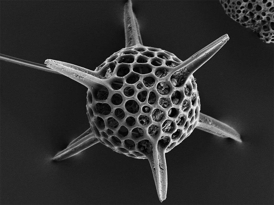
球体,")
球体,")


技术在Si/SiO2基材上生长的MoS2 2D晶体")
技术在Si/SiO2基材上生长的MoS2 2D晶体")


")
")
")
")
球体")
球体")


技术在Si/SiO2基材上生长的MoS2 2D晶体")
技术在Si/SiO2基材上生长的MoS2 2D晶体")
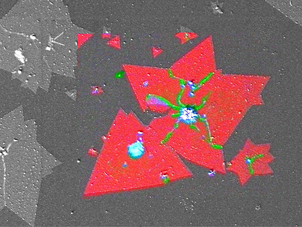


,突出了关键矿物中的地球化学分区。")
,突出了关键矿物中的地球化学分区。")
,突出了关键矿物中的地球化学分区。")
,突出了关键矿物中的地球化学分区。")


配件


蔡司FE-SEM原位实验室
连接材料性能与微观结构的桥梁
在进行加热和拉伸实验时,可通过使用原位解决方案来拓展蔡司FE-SEM,尽享集成解决方案的优势。对金属、合金、聚合物、塑料、复合材料以及陶瓷等材料进行深入研究。将力学拉伸或压缩载物台、加热单元和专用高温探测器与分析相结合。所有系统组件均可通过安装于个人电脑上的统一软件控制,从而实现无人值守的自动化材料测试。


SmartEDX
探索嵌入式能量色散X射线谱


完全集成的RISE
充分发挥拉曼成像和扫描电镜的性能优势
补充材料表征,并增加拉曼光谱成像。使用共聚焦拉曼成像功能,获取样品的化学指纹图并扩展您的Sigma 300。此外,它还可辨别分子和晶体信息,执行三维分析,将SEM成像与拉曼光谱成像和EDS数据相关联(如适用)。完全集成的RISE可充分发挥SEM和拉曼系统的全部优势。


 和 LA-ICP-MS 工作流程")
 和 LA-ICP-MS 工作流程")


