Extremely precise, extremely successful: 30 years of EUV lithography optics at ZEISS SMT
- EUV technology (extreme ultraviolet light) has evolved from a technology that was thought to be technically unfeasible into an industry standard
- A workshop in 1995 changed the future for digitalization and ZEISS SMT
- ZEISS SMT is already working on the next generation of lithography technologies for digital transformation
In 1995, an important milestone for the development of EUV lithography (extreme ultraviolet light) in Europe was a workshop at ZEISS Semiconductor Manufacturing Technology (SMT) in Oberkochen. Representatives from chip manufacturers and research institutes came together to shape the future of optical lithography. EUV lithography has revolutionized the semiconductor industry and is important for digital living and working.
The EUV lithography optics from ZEISS's SMT segment project the finest structures of under 10 nanometers onto wafers – thin silicon discs – using light with extremely short wavelengths of 13.5 nanometers. These optical systems, which can be described as the most precise mirrors with mechatronic systems for maximum stability are a crucial part of the EUV systems built by ASML. The systems are unique to ASML, ZEISS’ strategic partner, and enable smart technology.
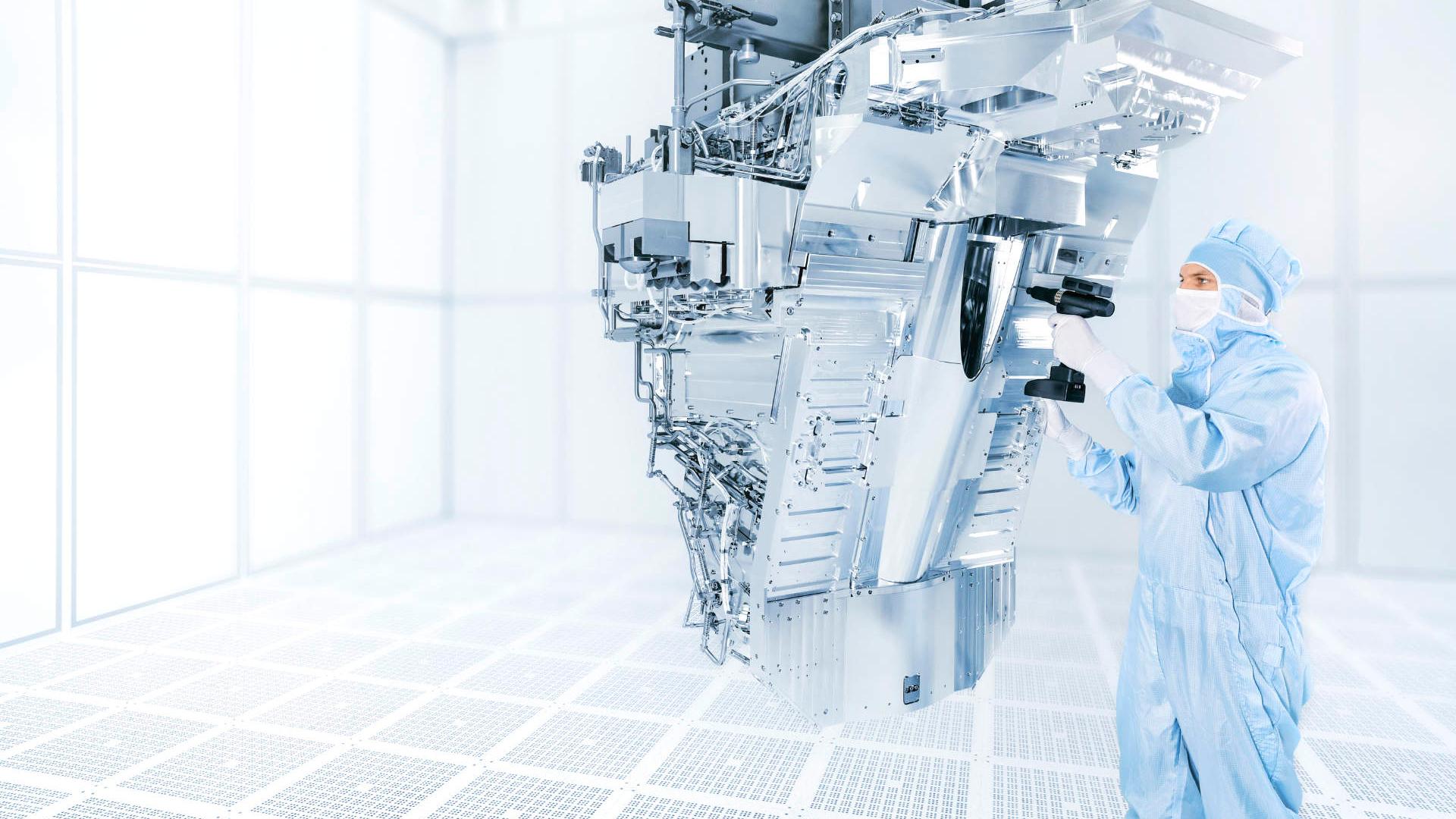

30 Years of EUV lithography optics: The ZEISS EUV illumination system consists of 15,000 individual parts and weighs 1.5 tons.
Pioneering spirit and perseverance lead to success
“Thirty years ago, EUV technology was considered visionary and technically unfeasible. Today, we carry this technology with us in every smartphone,” says Frank Rohmund, President and CEO of ZEISS SMT. The journey to this development was long: “EUV was not a self-runner. The feasibility of the technological leap was in question, as were the strategic and economic implications for future market positioning in the dynamic semiconductor market,” Rohmund explains. Thanks to a strong pioneering and team effort – comprising a network of more than 1,200 European partners – and intensive development work, the highly complex EUV technology has become a leading technology in chip manufacturing today.
Beyond the limits of what is technologically feasible
In EUV technology, precision and miniaturization are crucial criteria: The use of high-precision mirrors allows for stronger focusing of light and is essential for the miniaturization of integrated circuits. For this purpose, ZEISS has built the most precise mirrors in the world and positioned and aligned them with high accuracy in the optical system. “In this field, we are technology leaders,” says Christoph Hensche, Head of ZEISS Semiconductor Manufacturing Optics (SMO), a strategic business unit at ZEISS SMT. The result: Thanks to EUV, more than 57 billion transistors fit on the fingernail-sized silicon area of a microchip. “With EUV lithography, we have found a solution for the seemingly unsolvable problems and are the heartbeat and pacemaker of digitalization,” Hensche adds.
Looking ahead to the next technological leap
In the future, ZEISS will continue to empower semiconductor manufacturing to produce the next generation of microchips: “Starting in 2026, the first microchips are expected to be produced in series using High-NA-EUV lithography, the further development of EUV technology,” Rohmund states.


