Press Release

Innovative technologies for tomorrow: ZEISS at W3+ Fair in Wetzlar

5 March 2025
  • ZEISS SMT will be at the W3+ Fair in the Buderus Arena, Wetzlar on March 19 and 20, 2025 featuring its own booth
  • Insightful presentation on March 19 at 11 a.m. discussing the significant role of Central Hesse as a key region for the semiconductor industry
  • ZEISS leverages the expertise of Central Hesse, a leading hub for the optics industry, recognizing the region as essential for future growth
Wetzlar, Germany | 5 March 2025 | ZEISS Semiconductor Manufacturing Technology

The W3+ Fair, dedicated to optics, photonics, electronics, and mechanics, will open its doors once again on March 19 and 20, 2025. This year, the ZEISS segment Semiconductor Manufacturing Technology (SMT) will participate as a technology leader and key employer in the Central Hesse region. Attendees can find ZEISS at booth A11 in the Buderus Arena. Dr. Wolfram Hild, Project Manager R&D at ZEISS SMT, will give a presentation on March 19 at 11 a.m., highlighting the significance of Central Hesse as a key region for the semiconductor industry.

  • The picture shows a silicon wafer in which a person and a ZEISS Starlith 1700 are reflected.

    For more than 20 years, high-tech DUV lithography optics have been manufactured at the Wetzlar site in order to image ever smaller and more powerful structures on thin disk-shaped silicon discs - so-called wafers.

  • The picture shows the new multifunctional factory in Wetzlar’s ​​Dillfeld.

    The new multifunctional factory in Wetzlar's Dillfeld adds a production area of ​​more than 12,000 square meters to the existing site and offers space for around 150 employees.

Wetzlar: a cornerstone for future growth

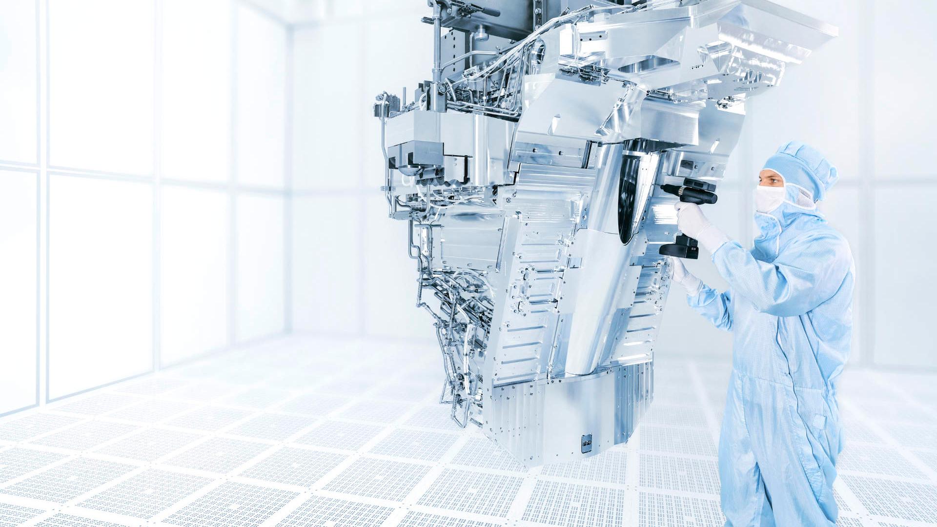
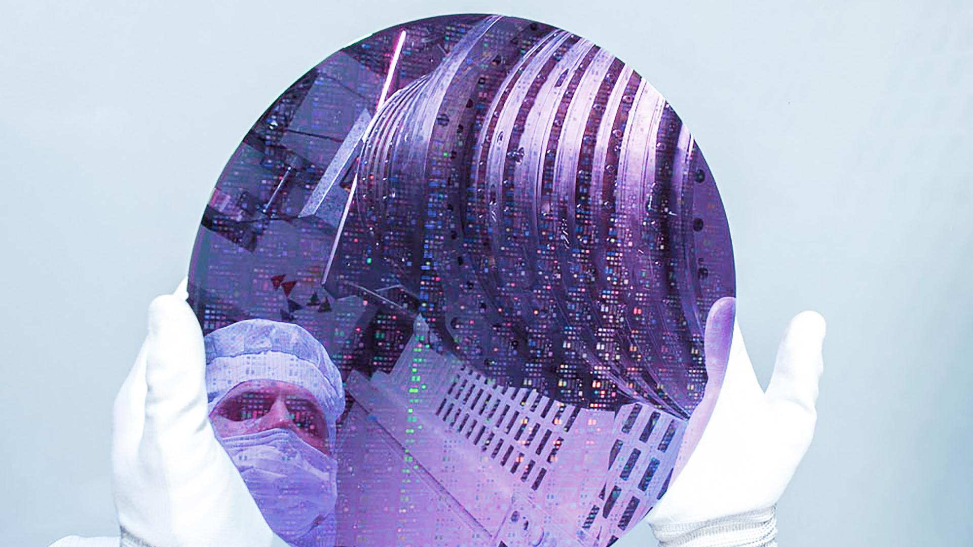
Approximately 80 percent of all microchips produced worldwide are manufactured using ZEISS SMT optics, providing a foundation for the continuation of Moore's Law. To achieve this, ZEISS capitalizes on Wetzlar's status as a premier center for the optics industry. “With their optical expertise and renowned research institutions Wetzlar and the Central Hesse region are vital to us as a technology company. We are committed to advancing technological progress in the region and investing in our company’s growth,” explains Katrin Ariki, Site Manager of ZEISS SMT in Wetzlar, emphasizing the region's importance.

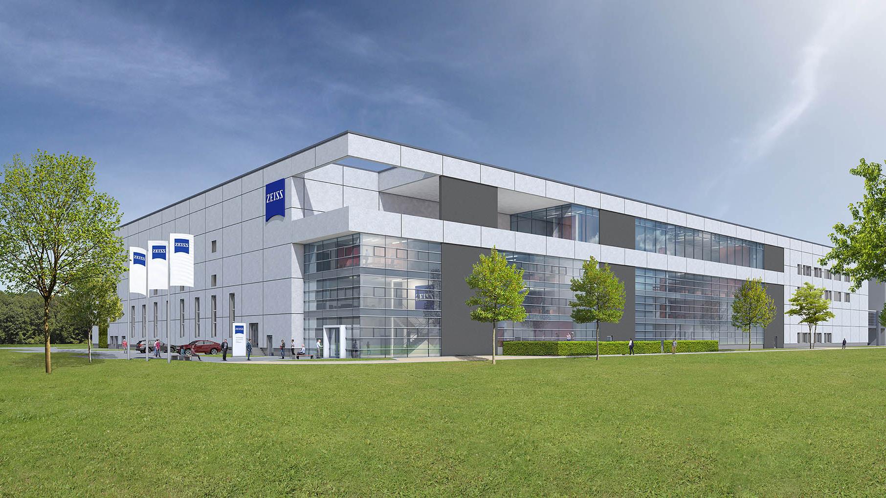
Last July, ZEISS celebrated a significant milestone with the topping-out ceremony of its new multifunctional factory in Wetzlar's Dillfeld (see press release). This expansion adds over 12,000 square meters of production space to the existing facility, providing optimal conditions for the production of DUV optics (DUV stands for "deep ultraviolet light"). This investment empowers ZEISS SMT to enable chip manufacturers worldwide to produce microchips with nanometer precision. It not only strengthens the region and the Wetzlar site as the "City of Optics" but also increases the demand for skilled professionals. For more than two decades, DUV lithography optics have been manufactured at the Wetzlar site, which currently employs around 500 professionals. To facilitate the next technological leap, ZEISS SMT is actively seeking specialists, particularly in development and production: “We are looking for talented individuals who want to contribute to a progressive future, as driving technological advancement requires innovative minds. We look forward to engaging and networking at the W3+ Fair,” says Ariki.

Portrait of Jeannine Rapp
Press Contact Jeannine Rapp Carl Zeiss SMT GmbH
Portrait of Jeannine Rapp
Press Contact Jeannine Rapp Carl Zeiss SMT GmbH

About ZEISS

ZEISS is an internationally leading technology enterprise operating in the fields of optics and optoelectronics. In the previous fiscal year, the ZEISS Group generated annual revenue around 11 billion euros in its four segments Semiconductor Manufacturing Technology, Industrial Quality & Research, Medical Technology and Consumer Markets (30 September 2024).

For its customers, ZEISS develops, produces and distributes highly innovative solutions for industrial metrology and quality assurance, microscopy solutions for the life sciences and materials research, and medical technology solutions for diagnostics and treatment in ophthalmology and microsurgery. The name ZEISS is also synonymous with the world's leading lithography optics, which are used by the chip industry to manufacture semiconductor components. There is global demand for trendsetting ZEISS brand products such as eyeglass lenses, camera lenses and binoculars.

With a portfolio aligned with future growth areas like digitalization, healthcare and Smart Production and a strong brand, ZEISS is shaping the future of technology and constantly advancing the world of optics and related fields with its solutions. The company's significant, sustainable investments in research and development lay the foundation for the success and continued expansion of ZEISS' technology and market leadership. ZEISS invests 15 percent of its revenue in research and development – this high level of expenditure has a long tradition at ZEISS and is also an investment in the future.

With over 46,000 employees, ZEISS is active globally in around 50 countries with more than 60 sales and service locations, around 40 research and development facilities, and 35 production facilities worldwide (30 September 2024). Founded in 1846 in Jena, the company is headquartered in Oberkochen, Germany. The Carl Zeiss Foundation, one of the largest foundations in Germany committed to the promotion of science, is the sole owner of the holding company, Carl Zeiss AG.

Further information at www.zeiss.com


Semiconductor Manufacturing Technology

With its product portfolio and expertise, the Semiconductor Manufacturing Technology segment of ZEISS covers a variety of key processes in the production of microchips. Its products include semiconductor manufacturing optics – notably lithography optics – as well as photomask systems and process control solutions for semiconductor manufacturing. Thanks to ZEISS technology, microchips are becoming increasingly smaller, more powerful, more energy-efficient and more affordable. The electronic applications of these ongoing enhancements enable global progress in many disciplines such as technology, electronics, communication, entertainment, mobility and energy. Semiconductor Manufacturing Technology is headquartered in Oberkochen. Other sites include Jena, Rossdorf, Wetzlar, Aachen and Coswig (Germany), Zurich (Switzerland), as well as Bar Lev (Israel) and Dublin, CA (USA).

Press Photos

  • For more than 20 years, high-tech DUV lithography optics have been manufactured at the Wetzlar site in order to image ever smaller and more powerful structures on thin disk-shaped silicon discs - so-called wafers.

    1 MB
  • The new multifunctional factory in Wetzlar's Dillfeld adds a production area of ​​more than 12,000 square meters to the existing site and offers space for around 150 employees.

    2 MB